Advanced Analysis of Bump Crack Formation Mechanisms in FPCB Manufacturing


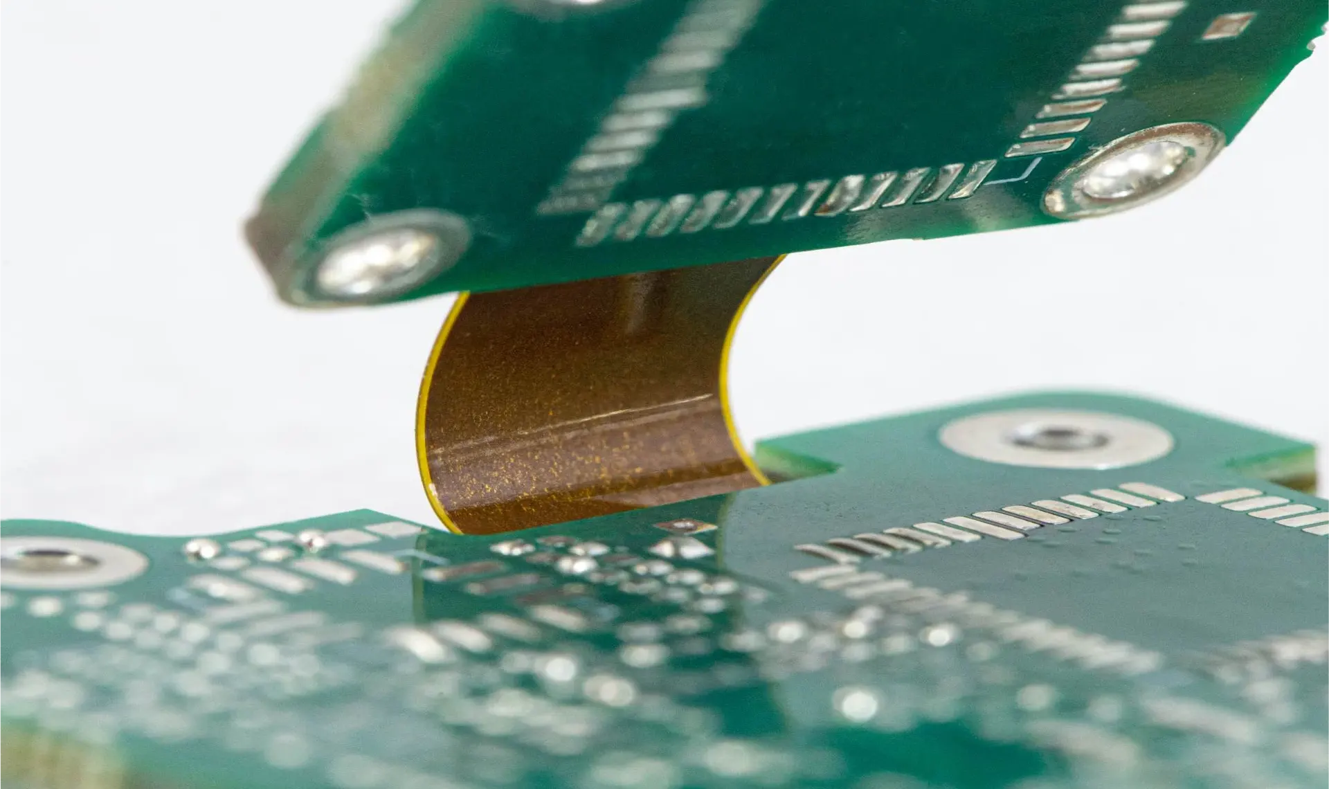
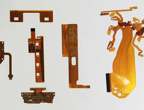
Flexible printed circuit boards (FPCBs) serve as the core components enabling flexible connections within electronic devices.
To ensure optimal contact between certain specialized devices and other components, bump technology is employed on FPCB connection pads.
Examples include applications such as the subscriber identity module (SIM) card slot in point-of-sale (POS) systems used for sales transactions, printer ink cartridges, and similar devices.
Bump reliability directly impacts product performance and lifespan, with FPCB bump cracking being a common failure mode during FPCB manufacturing, assembly, or operation.
This paper delves into the causes of bump cracking from engineering design, material selection, and stamping methods perspectives.
Bump Material Design
Bump Introduction
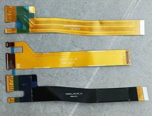
FPCB bump technology involves forming metal protrusions with specific height and shape at designated locations on the FPCB, as shown in Figure 1.

Figure 1 Physical View of the Connection Pad Bumps on the FPCB
These bumps play a critical role in providing electrical connections and mechanical fixation within electronic devices. Typically, local thickening of the material through stamping or electroplating creates raised areas at the center of connection pads. This paper primarily focuses on the application of stamping methods.
Design Requirements for Bump Connection Pads
To prevent copper foil tearing or collapse deformation during stamping, design the relationship between bump height (H), substrate thickness (T), and connection pad diameter (D) as shown in Figure 2. The specific requirements are as follows:
(1) When the bump height H exceeds 0.5 times the substrate thickness T, the connection pad diameter must satisfy D ≥ 1.8H. For example, if H = 0.30 mm, then D ≥ 0.54 mm.
(2) When the bump height H equals T, the diameter must satisfy D ≥ 2.5H. For example, if T = 0.10 mm, then D ≥ 0.25 mm.

Figure 2 Connection Pad Bumps on FPCB
Experiment 1: Effect of Connection Pad Design on FPCB Bump Cracking
Pad Dimension Constraints
Pad dimension constraints fall into two categories:
One type relies on copper foil, called copper-defined pads (CD Pad) or non-solder mask defined pads (NSMDP), commonly called ‘unprinted pads’ in FPCB design, as shown in Figure 3(a).
The other type relies on solder mask patterns, called solder mask defined pads (SMDP), commonly called ‘solder mask pads’ in FPCB design, as shown in Figure 3(b).
Since FPCBs use cover films instead of solder masks, this category further divides into cover film-defined pads and non-cover film-defined pads.

Figure 3 Dimensional Specifications for the Coupling Disc
Bump Pad Design
> Single-Sided FPCB Bump Pad Design
Design single-sided board pads as pressed pads, employing a specialized surface-mount device (SMDP) structure.
This design ensures the cover film fully compresses the area surrounding the connection pad, achieving a secure bonding effect. Its primary purpose is to prevent cracking or damage to the polyimide (PI) substrate during the raised pad stamping process, as shown in Figure 4.
Given that the PI thickness of FPCB substrates is typically only 25 μm, the area surrounding the connection pad becomes exceptionally fragile when the cover film fails to bond it effectively, due to lack of support. It is highly susceptible to cracking under mechanical stresses like stamping, thereby compromising product reliability and lifespan.

Figure 4 Single sided FPCB Connector Plate Design
> Double-Sided FPCB Connection Pad Design
The protruding side of the double-sided connector plate features a circular window design, while the recessed side is square, as illustrated in Figure 5.

Figure 5 Double-Sided FPCB Connector Plate Design
It is crucial to note that the dimensions of both sides of the connector plate and their windows must differ. Identical dimensions may cause the connector plate to detach. Testing of FPCBs at several manufacturing facilities validates this conclusion.
Pressed PAD Experimental Design and Results
To validate the impact of different bump connection pad designs on bump cracking, in-depth studies focused on two designs: pressed PAD and non-pressed PAD for the bump surface.
The experiments utilized 0.11 mm thick boards with 12 μm adhesive-free electrolytic copper, producing 16 pieces each. All stamped using the same steel die.
Twenty pads each were verified with and without pressure application during embossing. Results showed: 3 pads (15%) fractured in the pressure-applied design, while 17 pads (85%) fractured in the non-pressure-applied design.
Figure 6 shows the sample results.

Figure 6 Effect of Pressing vs. Not Pressing the Pad on Bump Formation
Experimental results indicate that cracks appeared in both pressure-applied and non-pressure-applied PADs.
However, the pressure-applied PAD design exhibited significantly fewer cracks than the non-pressure-applied PAD, and the cracks were relatively less severe.
Experiment 2: Effects of Electrolytic Copper and Rolled-Annealed Copper on Bumps
Introduction to Electrolytic Copper and Rolled-Annealed Copper
Electrolytic (ED) copper forms by depositing copper ions onto a cathode drum in a copper sulfate electrolyte, producing copper foil with a columnar crystalline structure. It offers low production costs, mature manufacturing processes, and suitability for mass production [1].
Rolled-annealed (RA) copper forms by repeatedly hot-rolling, cold-rolling, and annealing high-purity copper ingots. It features a horizontal layered grain structure and excellent ductility. However, its manufacturing process is complex, requires high equipment precision, and incurs significantly higher costs than ED copper [2].
Copper Foil Type Experimental Design and Results
The experiment utilized 0.11 mm thick sheets of 12 μm adhesive-free electrolytic copper and rolled copper. All test specimens employed a pressed PAD design, with 16 pieces per group stamped using the same steel die set.
Twenty embossed points were verified on both electrolytic copper and rolled copper pads. Results showed: 4 embossed points (20%) fractured in electrolytic copper, while none fractured (0%) in rolled copper, with all rolled copper samples passing.
Experiment 3: Impact of Different Stamping Dies on Embossed Points
Stamping Die Introduction
Stamping dies for raised pads primarily consist of Bakelite board dies and steel dies, as shown in Figure 7.
")
Figure 7 Phenolic Board Fixture and Steel Mold (Actual Items)
Bakelite board dies offer low processing costs, suitable for low-cost or single-use scenarios. Steel dies, though higher in processing cost, prove more economical during mass production as costs spread over multiple uses. Table 1 details the specific characteristics of both

Table 1 Differences Between Bakelite Board Fixtures and Steel Molds
Experimental Protocol and Results for Different Die Materials
The test utilized 0.11mm thick, 12 μm adhesive-free rolled copper sheets. All test samples featured a pressed PAD design, with 16 pieces per group. Each group stamped using either a bakelite die or a steel die.
During verification, both molds stamped 20 copper-clad laminate pads. Results showed: 4 pad fractures (20%) occurred with the Bakelite mold, featuring sharp and rough fracture edges; no fractures (0%) occurred with the steel mold, with all steel molds passing inspection.
Conclusions
This experiment investigated the impact of three factors—engineering data design, copper foil type, and stamping dies—on crack formation in FPCB connection pad bumps. The following summarizes the findings:
(2) Rolled copper is recommended over electrolytic copper due to the latter’s inherent risk of bump cracking.
(3) Bakelite jigs suit sample production, while steel dies support mass manufacturing.
This experiment preliminarily validated key control points for FPCB bump connection pads. However, numerous factors remain unaddressed, including differences between single- and double-sided boards, the impact of copper thickness on bump cracking, distinctions between adhesive-free and adhesive-backed substrates, and variations in supplier materials. Further discussion and in-depth study with industry process technicians remain encouraged.