PCB Testing: 8 Essential Methods for Quality Assurance (2025 Update)


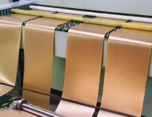
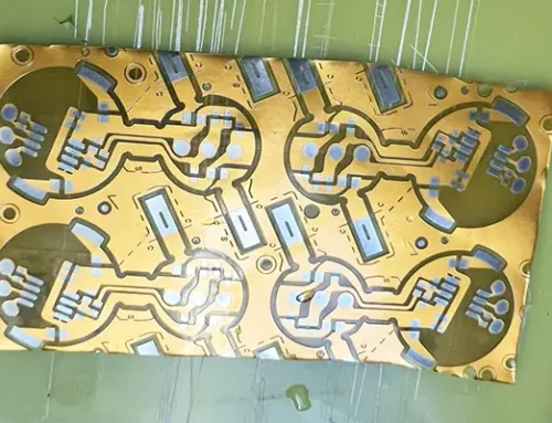
Printed circuit boards (PCBs) are essential components for all electronic products. Manufacturers use them in smartphones, medical devices, computers, and military equipment. As PCBs become more complex with high densities, fine pitches, and multilayers, full test coverage is crucial. This helps protect against hidden defects and ensures steady manufacturing yields.
In today’s post, we will explore 8 common PCB testing methods. We will examine what they are, their common uses, and their advantages and disadvantages. We will also discuss why these methods are still important in PCB manufacturing. These techniques help check if your PCB performs well and meets design specifications.
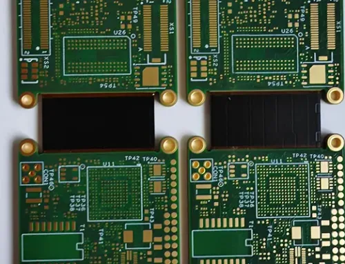
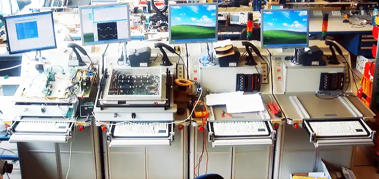
1. AOI (Automated Optical Inspection)
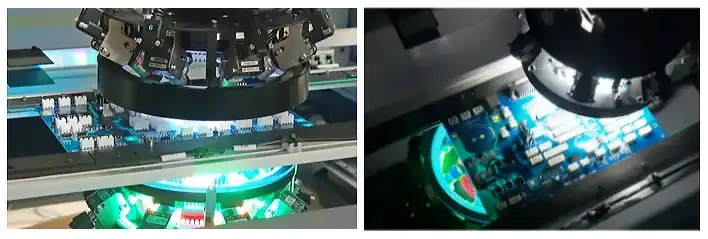
Taking top-and-bottom AOI. Images courtesy of MEK Marantz Electronics
AOI machines use high-resolution cameras to find surface-mounting errors. These errors include solder bridges, missing parts, and misalignment.
Scan after solder paste printing or reflow soldering in SMT assembly.
Advantage: Fast, non-contact, ideal for high-volume lines
Limitation: Cannot detect internal defects (e.g., via voids)
Reference:
Automated Optical Inspection (AOI), Apps, and Machine Learning: Tools for PCB Quality Control
2. In-Circuit Testing (ICT)
ICT involves electrical probes that test individual components on a PCB assembly for shorts, opens, and component values.
Best for: Mass production, especially in rigid or flex-rigid boards
Tools: Bed-of-nails fixture, test access via PTH holes
Limitation: Costly fixture setup for small-batch runs
Reference:
How In-Circuit Tests Ensure PCBA Quality and Reliability
3. Flying Probe Testing
Flying probes work similarly to ICT but do not utilize a fixed test bed. They move across the board to check netlist connections and basic component values.
Advantage: Low setup cost, flexible for prototypes, and low-volume PCB assembly
Limitation: Slower than ICT; limited by access points
4. Boundary Scan (JTAG Testing)
For complex digital boards, boundary scan testing lets embedded parts test each other. You perform this through a serial test access port.
Application: BGA-heavy designs, high-density interconnect PCBs (HDI PCBs)
Advantage: Ideal for testing inaccessible areas
Limitation: Requires JTAG-compatible devices
Reference:
Boundary Scan Tutorial
5. X-ray Inspection (AXI)
Automated X-ray Inspection checks for hidden defects beneath BGA packages and inside multilayer PCBs.
Detects: Cold solder joints, voids, internal misalignments
Used in: Medical, military, and aerospace boards
Limitation: Expensive equipment; typically post-reflow
6. Functional Testing (FCT)
FCT Test
Functional tests simulate real-world conditions to validate board performance under load.
Benefit: End-to-end validation of assembled PCB
Used for: Final test phase before shipment
Tools: Custom test jigs, software simulators
Reference:
Functional Circuit Test (FCT) – A Basic Introduction Is Here – NextPCB
7. Visual Inspection
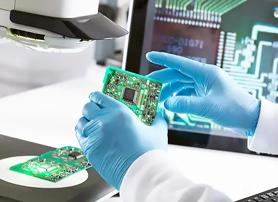
Visual Inspection
While basic, manual inspection still plays a role, especially for prototype PCBs, double-sided boards, and connector zones.
Used in: Low-budget setups or quick QA checks
Tips: Combine with checklists or smart magnification tools
Reference:
The essentials of manual visual inspection in PCB manufacture
8. Environment & Burn-In Testing
Burn-in involves running a board under stress conditions (high temp/load) to screen for early failures.
Used in: Automotive, military, or mission-critical applications
Test types: Thermal cycling, humidity, vibration, high-voltage
Choosing the Right PCB Test Strategy
The right test combination depends on:
- Board type: rigid, flexible PCBs, rigid-flex PCBs
- Production volume: prototype vs. mass production
- Application risk: consumer vs. industrial/medical
- Layer complexity: single-sided, double-sided, or multilayer PCB
Integrating effective testing ensures fewer defects, lower returns, and a stronger market reputation.
Conclusion
Using the right testing strategy is essential. This applies whether you are making flexible FPC boards, high-speed HDI circuits, or standard single-sided assemblies. This helps ensure your products perform consistently.
Need help designing or validating your PCB test flow? Gekun provides end-to-end PCB solutions, from design to SMT to testing. Get in touch with our engineering team today.
FAQ:
1. Why is PCB testing important in modern electronics manufacturing?
As PCBs become more complex—with higher densities, fine-pitch components, and multilayer designs—testing is crucial to detect hidden defects, maintain stable manufacturing yields, and ensure the final product meets performance and reliability specifications. Effective testing reduces failures, returns, and field issues.
2. What is the difference between AOI and X-ray inspection?
AOI (Automated Optical Inspection) uses high-resolution cameras to detect surface defects such as missing components, solder bridges, or misalignment. It is fast and ideal for high-volume SMT lines.
X-ray inspection (AXI), however, can detect hidden or internal defects—such as voids, BGA solder issues, and internal misalignments—that AOI cannot see. AXI is more expensive and typically used for high-reliability boards.
3. When should I use In-Circuit Testing (ICT) vs. Flying Probe Testing?
Use ICT when:
You have mass production
Boards have accessible test points
You need fast, high-coverage testing
Use Flying Probe when:You are building prototypes or low-volume batches
You want to avoid high fixture costs
Your design changes frequently
ICT is faster but more expensive to set up; flying probe is slower but highly flexible.
4. What is Boundary Scan (JTAG), and when is it needed?
Boundary Scan (JTAG) allows embedded ICs to test interconnects through a serial interface. It is essential for:
HDI boards
BGA-dense layouts
Areas where test probes cannot reach
Its limitation is that all participating devices must support JTAG.
5. What is Functional Testing (FCT), and why is it used?
Functional Testing simulates real operating conditions to verify the fully assembled PCB behaves exactly as designed. It checks power-up behavior, signal response, interfaces, and safety requirements. FCT is typically the final test stage before shipment and helps catch faults that electrical or optical tests may miss.
6. What types of PCB tests are required for high-reliability applications?
Sectors such as automotive, aerospace, defense, and medical devices typically require:
AXI (X-ray) to check internal structures
Burn-in and environmental tests (thermal cycling, humidity, vibration)
FCT to ensure the board works under real-world load
These stress tests help identify early failures and ensure long-term reliability in mission-critical applications.