PTFE Blind Via Processing for High-Frequency FPC: Process Optimization and Insertion Los


Industry Background and Technology Trends
With the rapid advancement of artificial intelligence, 5G communications, and IoT technologies, electronic devices are rapidly evolving toward higher frequencies, faster speeds, miniaturization, and integration.
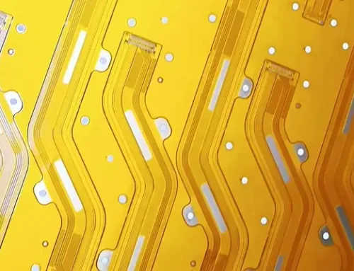
Against this backdrop, high-frequency flexible printed circuit boards (FPCs), as critical interconnect components, face increasingly stringent performance requirements.
Signal transmission integrity and low-loss characteristics have become key factors determining device performance.
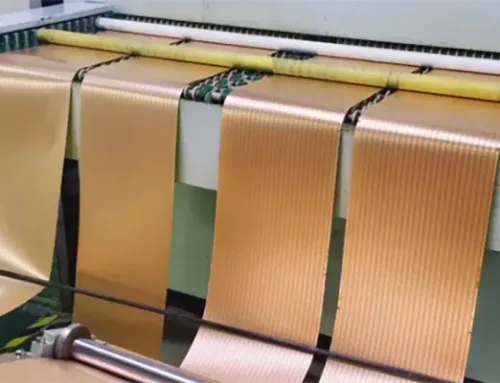
High-Frequency FPC Material Systems
Current high-frequency FPC material systems primarily encompass three major categories: modified polyimide (MPI), liquid crystal polymer (LCP), and polytetrafluoroethylene (PTFE) .
Among these, PTFE materials are the preferred choice for high-frequency applications due to their outstanding dielectric properties (low dielectric constant and low loss factor).
However, their poor processability and narrow process window pose significant challenges in actual production.
Blind Via Processing Challenges in PTFE
As a critical structure for achieving high-density interconnects, the processing quality of blind vias directly impacts signal transmission loss and impedance matching characteristics.
PTFE materials typically contain components such as glass fibers and ceramic fillers, which increase the difficulty of blind via processing.
Electroplating of blind vias in PTFE materials is another processing challenge. Currently, common pre-plating pretreatment processes for FPCs include black shadowing, black hole treatment, and copper plating.
Research Gap and Study Focus
Each has distinct process characteristics (copper plating is indicated by a horizontal line, as shown in Table 1), but research on the relationship between these three processes and insertion loss remains relatively scarce.
Therefore, this paper focuses on PTFE materials to introduce blind hole processing techniques while investigating the impact of black shadow, black hole, and copper plating processes on product functionality, aiming to provide reference for PTFE blind hole processing.
Process characteristics (electroless copper plating is indicated by horizontal lines, as shown in Table 1), but research on the relationship between these three processes and insertion loss remains relatively scarce.
Comparison Item | Graphite Shadowing | Carbon Black Hole | Electroless plating copper (PTFE Material) |
|---|---|---|---|
Process Design | Loading → Clean graphite tank #1 → Rinse → Graphite tank #1 → Fixation tank #1 → Rinse → Dryer #1 → Microetch #1 → Rinse → Intermediate inspection → Clean graphite tank #2 → Rinse → Graphite tank #2 → Fixation tank #2 → Rinse → Dryer #2 → Intermediate inspection → Microetch #2 → Rinse → Anti-oxidation → Rinse → Dryer → Unloading | Loading → Cleaning → Rinse → Carbon black tank #1 → Cold air blow → Dryer #1 → Intermediate inspection → Graphitization → Rinse → Carbon black tank #2 → Cold air blow → Dryer #2 → Intermediate inspection → Microetch → Rinse → Anti-oxidation → Rinse → Dryer → Unloading | Loading → Degreasing → Rinse → Microetch → Rinse → Acid dip → Rinse → Pre-dip → Activation → Rinse → Acceleration → Rinse → Chemical copper → Rinse → Drying → Unloading (According to product requirements, two chemical copper treatments may be needed) |
Core Principle | Physical adsorption of graphite | Physical adsorption of carbon black | Chemical copper plating |
Conductive Material Properties | Flake graphite, particle size 300–700 nm, non-oxidizing | Granular carbon black, particle size 80–140 nm, non-oxidizing | Chemical copper, easily oxidized |
Electrical Conductivity | Better than carbon black, weaker than chemical copper | Weaker than graphite and chemical copper | Better than graphite and carbon black |
Environmental Performance | Environmentally friendly | Environmentally friendly | Contains formaldehyde, complexing agents, heavy metals |
Main Tank Service Life | 1 year | 6 months | Activation: 1 month; Chemical copper: 15–30 days |
Equipment Length | ~28 m (at 2 m/min) | ~24 m (at 2 m/min) | ~34 m (at 2 m/min) |
Based on this, this paper focuses on PTFE materials as the research subject, introduces its blind via processing technology, and simultaneously investigates the impact of black shadow, black hole, and electroless copper plating processes on product functionality.
It is hoped that this will provide reference for blind via processing of PTFE materials.
Test Design
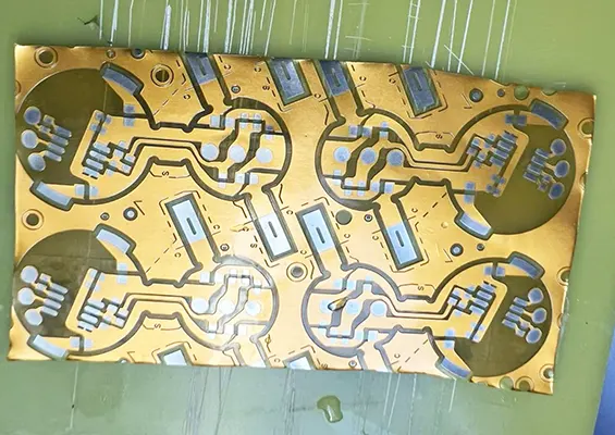
Test Coupon Design
The test coupon was designed as a double-sided board with PTFE substrate and a 75 μm dielectric layer, featuring blind vias with a 100 μm aperture. The laminate structure is shown in Figure 1.

Figure 1. Test coupon overlay diagram
Test Coupon Process Flow
Cutting → Dry film circuit pattern → Etching → Laser blind via drilling → High-pressure water washing → PLASMA → Black shadow/Black hole/Electroless copper plating → Flash plating → Via filling plating → Dry film circuit pattern → Etching → AOI → Cover film lamination → Chemical gold plating → Characterization → Reinforcement lamination → Electrical testing → Forming
Test Equipment
Metallurgical microscope, 3D microscope, scanning electron microscope, impedance meter, vector network analyzer.
Process Testing
Laser Blind Via
The substrate used for this test coupon is PTFE resin containing glass fiber and ceramic fillers.
PTFE exhibits excellent thermal stability with a complete carbonization temperature of approximately 500–600°C. However, ceramic fillers in the substrate cause refraction and scattering of the laser beam, reducing the efficiency of energy absorption within the PTFE resin and leading to uneven carbonization.
This significantly increases the processing difficulty of laser blind hole drilling in PTFE substrates, making the design of a reasonable laser blind hole processing scheme particularly important.
Given extensive existing research on laser blind hole processing of PTFE substrates, this paper will not elaborate on the relationship between laser processing schemes and blind hole formation, but will briefly share results.
The test employed a CO₂ + UV laser combination (non-integrated system) for laser blind-hole processing of PTFE. The CO₂ laser primarily removes the PTFE resin layer, while the UV laser performs bottom hole cleaning. Before laser processing, the substrate underwent etching for windowing.
If etching for windowing is omitted and CO₂ laser processing is applied directly, the copper surface requires burnishing.
This process significantly increases copper surface roughness, potentially interfering with high-frequency signal insertion loss test results.
While switching to UV laser windowing avoids roughness issues, its alignment accuracy is inferior to the etching process. Laser blind hole processing parameters are shown in Table 2.
Combined with the observations in Figure 2, this process achieves excellent quality: microscopic inspection confirms intact copper layers at the blind hole bottoms with no residual adhesive.

Table 2 Laser Drilling Parameters

Figure 2
Follow-up studies will supplement cross-sectional analysis after blind hole plating and thermal stress testing (288°C, 10 s, 3 cycles). All test results indicate that the current laser blind hole solution meets the requirements for this test.
Hole Metallization
PTFE consists of C-F bonds, exhibiting extremely low surface energy and lacking reactive functional groups. This makes it difficult for metal plating to adhere.
Additionally, PTFE material is hydrophobic, hindering the wetting of its surface by electroplating solutions.
Therefore, blind hole walls must first undergo modification via PLASMA activation to facilitate subsequent hole metallization. PLASMA parameters are shown in Table 3.

Table 3 PLASMA Parameter Table
After PLASMA treatment, the boards undergo shadowing, black hole treatment, and copper plating. The treated boards then proceed to flash plating + via filling (full-board plating).
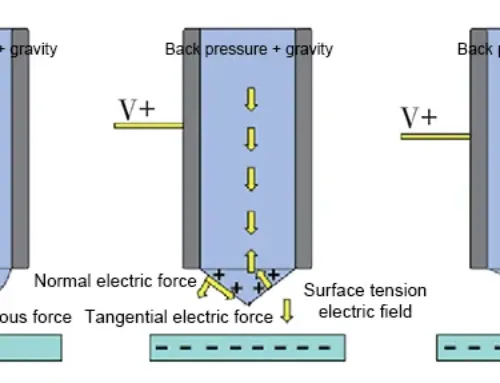
Cross-sections of the blind vias after plating are examined (as shown in Figure 3). No ICD was detected in the blind vias treated by any of the three processes, with dimple values <5μm, meeting the test requirements.

Figure 3 Comparison of blind hole electroplating
Validation Testing
Roughness Testing
Under high-frequency testing conditions, signal transmission in FPCs tends toward the conductor surface. The relationship between skin depth and signal frequency is shown in Figure 4.

Figure 4. Relationship between skin depth and testing frequency
As illustrated, higher test frequencies exhibit greater sensitivity to conductor surface roughness.
› Roughness Measurement at Key Process Nodes
Surface roughness analysis was conducted using a 3D microscope on test coupons processed with black shadow, black hole, and electroplated copper techniques.
Testing covered three critical process nodes: post-via plating, post-dry film micro-etching, and post-cover film micro-etching (both micro-etching processes employed sulfuric acid + hydrogen peroxide systems). Test data are shown in Table 4, revealing that:

Table 4 Roughness Test Comparison
The copper surface roughness of the three processes after via plating was essentially consistent, showing no significant differences.
After micro-etching, the copper surface roughness of all samples exhibited an upward trend.
It is particularly important to note that during actual mass production, the thin thickness of the CCL substrate and the inherent low rigidity of PTFE material make it highly susceptible to mechanical crease defects during process handling and machining.
Such defects can cause abnormal increases in copper surface roughness in localized areas, thereby affecting high-frequency signal transmission performance.
Therefore, strict control of panel flatness is essential when processing PTFE materials.
› Influence of Flash Plating on Surface Morphology
Before via filling plating, a flash plating step is performed. Roughness tests conducted on boards treated with black hole and electroless copper processes after flash plating are shown in Figure 5.
Results indicate that boards treated with the black hole process exhibit significantly lower copper surface roughness than those treated with electroless copper.
This is because the black hole process incorporates a micro-etching step in the latter part of the horizontal line, effectively removing residual carbon black conductive layers from the board surface.
This preserves the low roughness characteristic of the original copper substrate, maintaining a relatively smooth surface state after flash plating (the same principle applies to the black shadow process).
In contrast, the electroless copper process deposits a chemically formed copper layer with a relatively coarse microscopic structure on the copper surface.
Since the flash plating layer is thin (approximately 4 μm), it is insufficient for leveling, resulting in the copper surface retaining a relatively high roughness after the electroless copper + flash plating treatment.
During the subsequent via-filling electroplating process, increasing the copper plating thickness uniformly evens the copper surface roughness.

Figure 5. Roughness comparison after flash plating
Impedance Testing
Impedance testing took place on test coupons processed using three distinct techniques—black shadow, black hole, and electroplated copper—using an impedance tester. Figure 6 shows the test results.
Data analysis shows that the measured impedance values under all three process conditions consistently remain within ±6% tolerance of the target impedance. This result fully validates the stability of the different manufacturing processes.

Figure 6 Impedance test values
Insertion Loss Testing
Insertion loss testing took place on test coupons processed using shadowing, black hole, and plated-through copper techniques using a vector network analyzer. Test frequencies covered 6 GHz, 10 GHz, 20 GHz, 30 GHz, and 40 GHz (reaching the testing equipment’s limit).
Figure 7 shows the test results. Data analysis indicates that below 40 GHz, no significant differences in insertion loss performance appeared among the three processes.
This primarily results from consistent key parameters across all processes, including substrate thickness, cover film thickness, and conductor surface roughness.
However, as the test frequency increases, insertion loss variations between different batches gradually widen.
This phenomenon arises from heightened sensitivity of signal transmission to conductor surface roughness at high frequencies. Inherent variations in micro-morphology (e.g., roughness fluctuations) between batches lead to increased dispersion in high-frequency insertion loss performance.
Reliability Testing
Test coupons processed via shadowing, black hole, and electroplated copper techniques underwent tin-plating tests (288°C, 10 s, 3 cycles).
This test simulates extreme thermal shocks that FPCs may encounter during subsequent assembly (e.g., lead-free reflow soldering) or maintenance, evaluating the bonding strength between the plated hole metallization layer and substrate, as well as the coating’s resistance to thermal stress (e.g., delamination, cracking).
Observation via metallographic microscopy and SEM cross-sections (as shown in Figure 8) revealed no defects (such as delamination, cracks, or hole wall separation).
This indicates that the hole metallization structures formed by all three processes exhibit excellent thermomechanical reliability, meeting the requirements of the tin-plating test.

Figure 7

Figure 8 Thermal stress test slice
Conclusion
This study evaluated three processes—black shadow, black hole, and copper plating—for blind hole processing in PTFE materials, assessing their impact on product functionality. Conclusions are as follows:
(1) CO₂ + UV combined processing is recommended for laser blind holes in PTFE to enhance hole bottom cleanliness;
(2) PTFE requires plasma activation treatment before hole metallization;
(3) Shadowing, black holes, and electroplated copper all form conductive layers on the hole walls without affecting subsequent electroplating processes. Post-plating surface roughness of the copper layer showed no differences among these methods.
(4) Products processed via shadowing, black holes, or electroplated copper exhibited identical insertion loss performance below 40 GHz and all passed the tin-floating test.
We hope these conclusions provide a valuable reference for colleagues processing PTFE materials.