Precision Laser Soldering for FPCBs: Low Heat, High Reliability in Wearables and Medical Electronics


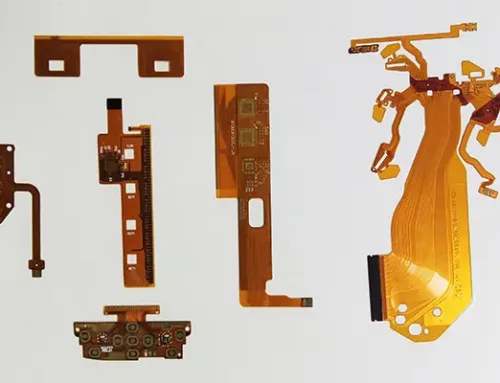
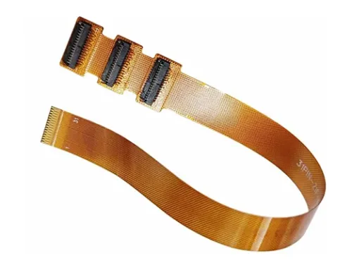
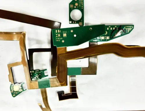
In fields such as consumer electronics, medical electronics, and wearable devices, flexible printed circuit boards (FPCBs) have become the core medium for achieving product miniaturization and structural innovation due to their characteristics of being lightweight, thin, bendable, and resistant to repeated bending.
However, the substrate materials of Flex PCBs (such as PI film and PET film) exhibit poor heat resistance (typically ≤150°C), and the copper foil traces are thin (mostly 12-35μm thick).
Traditional soldering methods (e.g., iron soldering, hot-air soldering) create large heat-affected zones (HAZ ≥ 200 μm) and localized high temperatures (exceeding 200°C), often resulting in substrate shrinkage/deformation, copper foil delamination, and circuit breakage.
Defect rates commonly reach 8%-12%, severely limiting Flex PCB reliability and lifespan.
Laser solder ball bonding solutions now exist, centered on “localized precision heating + low HAZ control.” Through three technological innovations—laser source optimization, closed-loop energy control, and non-contact welding—the HAZ in FPCB bonding is strictly confined to under 50 μm, with a substrate temperature rise of ≤30℃. reducing copper foil delamination rates below 0.1% while achieving stable yield rates exceeding 99.6% for 0.15mm micro-solder joints.
This article explores how precision welding technology safeguards FPCB flexibility through three dimensions: substrate protection challenges in FPCB welding, technical details of laser solder ball welding’s low heat-affected zone, and real-world application cases.
Core Challenges in Substrate Protection During FPCB Soldering: Thermal Damage Dilemmas of Traditional Processes
The structural characteristics and material limitations of FPCBs make “thermal control” during soldering a critical challenge. Traditional soldering processes face insurmountable constraints in three dimensions—heat-affected zone (HAZ), temperature precision, and mechanical pressure—directly threatening substrate integrity.
(1) Excessive Heat-Affected Zone: Primary Cause of Substrate Deformation and Copper Foil Delamination
Conventional heating methods fail to concentrate energy, resulting in heat-affected zones far exceeding FPCB tolerance limits:
Soldering Iron:
Direct contact between the iron tip and FPCB causes heat to spread via conduction, creating a HAZ of 300-500μm. PI film undergoes irreversible shrinkage (over 5%) at high temperatures, reducing trace spacing and potentially causing short circuits.
Simultaneously, high temperatures degrade the adhesive bonding the substrate to copper foil, causing foil delamination exceeding 10% and severely compromising circuit conductivity;
Hot-air soldering:
Hot air provides planar heating with a heat-affected zone ≥200μm.
Temperature fluctuations in the hot air stream can reach ±15℃. Even with a set temperature of 180℃, localized hot spots may exceed 200℃. This causes the FPCB’s cover film (if its temperature tolerance ≤160℃) to bubble, peel off, and lose its insulating protective function.
(2) Inaccurate Temperature Control: Circuit Damage Caused by Localized Overheating
FPCB copper traces are thin and dissipate heat rapidly. Traditional processes lack sufficient temperature control precision, often resulting in dual issues of “localized overheating” or “insufficient heating”:
Localized Overheating:
To ensure complete solder melting, traditional processes often require elevated soldering temperatures (e.g., iron set to 280-320°C).
Concentrated heat around solder joints causes copper trace oxidation (oxidation layer ≥1μm), increasing impedance by over 30% and impairing signal transmission efficiency.
Some fine traces (line width ≤50μm) may even melt and break due to excessive heat, directly causing product scrap.
Insufficient heating:
Lowering temperatures to avoid thermal damage results in incomplete solder melting, poor wettability at joints, and a false connection rate exceeding 8%.
During subsequent Flex PCB bending, joints are prone to fracture due to stress concentration, leading to persistently high product rework rates.
(3) Mechanical Pressure Damage: Physical Degradation of Flexible Substrates
Flex PCB substrates are flexible with low resistance to mechanical stress. Mechanical pressures from traditional contact-based soldering processes directly damage the substrate:
Soldering iron contact pressure:
Soldering tips require 50–100g of pressure for heat transfer. Flex PCBs easily develop indentations (depth ≥20μm) under pressure, compromising the substrate’s flexible structure and reducing bend resistance.
Wire-feeding pressure in wire-feeding soldering:
When the wire-feeding mechanism delivers solder wire to the joint, it generates 20-30g of lateral pressure. Thin FPCBs (thickness ≤0.1mm) are prone to deformation, causing joint positional shifts and increasing bridging risks by 5%;
Fixture clamping pressure:
To prevent FPCB displacement during soldering, traditional equipment applies clamping pressure via fixtures. Uneven pressure can cause localized wrinkling of the substrate, compromising subsequent assembly precision.
Low Heat-Affected Zone Technology in Laser Solder Ball Bonding: Three Major Innovations Safeguard FPCB Substrates
Addressing the critical challenge of substrate protection in Flex PCB bonding, the laser solder ball bonding solution achieves breakthroughs across three dimensions—“energy focusing, temperature precision, and non-contact operation”—to establish a low heat-affected zone technology system.
This approach ensures joint quality while maximizing preservation of the Flex PCB’s flexible properties.

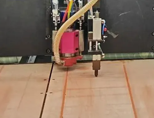
Laser Solder Ball Welding Machine
(1) Laser Light Source Optimization: Short-Wavelength Laser Enables “Surface-Focused Heating”
Laser wavelength directly determines energy absorption and penetration depth. Selecting wavelengths optimized for Flex PCBs reduces heat diffusion into substrates at the source:
Surface Heating Advantage:
Short-wavelength lasers concentrate energy on the Flex PCB surface (penetration ≤1μm), acting only on solder balls and copper pads while preventing heat transfer to PI film substrates. Ultraviolet lasers, with their high photon energy, directly act on the solder surface to achieve a “cold soldering” effect.
The heat-affected zone can be controlled within 30-40μm, which is 1/3 to 1/4 that of infrared lasers.
Precise laser spot focusing:
Through our proprietary optical focusing system, the laser spot diameter is minimized to 50μm. Combined with 5-megapixel sub-pixel visual positioning (±0.003mm accuracy), this ensures laser energy covers only the pad area without affecting surrounding circuits or substrates.
Controlling the spot diameter at 80 μm when soldering a 0.15 mm pad concentrates heat entirely within the pad without causing significant temperature rise in the surrounding PI film.
Multi-wavelength adaptation for different Flex PCB types:
Selecting a 450 nm blue laser for thick copper foil Flex PCBs (copper thickness ≥35 μm), which absorbs 65% of blue light, ensures thorough pad heating. Employing a 355 nm ultraviolet laser for thin copper foil Flex PCBs (copper thickness ≤12 μm) melts solder with lower energy, further minimizing the heat-affected zone.
(2) Energy Closed-Loop Control: Pulse Heating and Real-Time Temperature Control Prevent Overheating
Precise laser energy regulation is critical for controlling the heat-affected zone. A closed-loop system combining “pulse heating + real-time temperature feedback” enables fine-grained energy distribution to prevent heat accumulation:
Pulse-Interval Heating Process:
Utilizing pulse mode, each heating cycle melts only the solder ball. During the cooling phase, heat rapidly dissipates, allowing the Flex PCB substrate ample time to cool and preventing temperature escalation caused by heat accumulation. Controlling single heating pulse energy at 5–8 J when soldering SAC305 solder balls (melting point 217 °C) ensures solder melting while limiting substrate temperature rise to under 30 °C.
Real-time Infrared Temperature Feedback:
Equipped with a high-sensitivity infrared temperature sensor (sampling frequency 10,000 times/second, measurement accuracy ±1°C), it continuously monitors temperature changes around the Flex PCB pads.
If substrate temperature approaches 120°C (the safety threshold for PI film), laser power is immediately reduced or cooling time extended to maintain the substrate within the safe temperature range.
(3) Non-contact welding: Preserving FPCB flexibility without mechanical stress
FPCBs exhibit low resistance to mechanical stress. The non-contact soldering method of laser solder ball welding fundamentally eliminates the mechanical damage inherent in traditional processes:
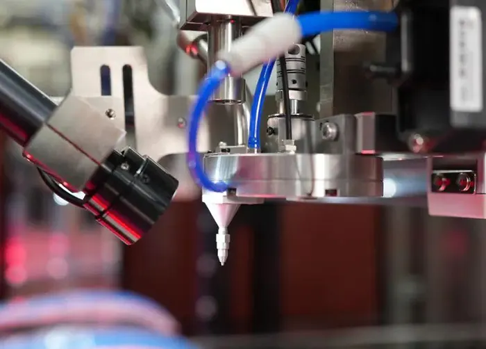
Solder Ball Jet Welding:
Propelling molten solder balls onto Flex PCB pads via nitrogen pressure requires zero mechanical contact.
This prevents substrate indentation caused by soldering iron tips or wire-feeding mechanisms. Spray pressure is precisely adjustable (0.2-0.5MPa).
Applying low pressure (0.2–0.3 MPa) to thin Flex PCBs (≤0.1 mm thickness) ensures full solder wettability while preventing substrate deformation.

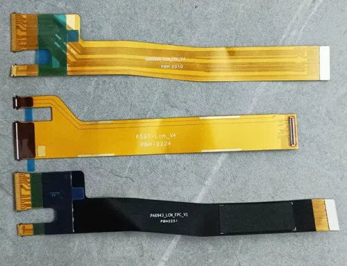
Solder Ball
Suspension-based positioning design:
Replaces traditional fixture clamping with visual positioning. A 5-megapixel camera captures reference points on the Flex PCB, dynamically adjusting the soldering position in real time. This eliminates fixture pressure, preventing substrate wrinkling.
For large-area Flex PCBs (dimensions ≥100mm×100mm), a vacuum suction platform (suction pressure ≤0.05MPa) provides flexible fixation that prevents displacement without damaging the substrate;
3D Welding for Curved Structures:
The multi-axis motion platform for laser solder ball welding (X/Y/Z-axis repeatability ±0.002mm) enables multi-angle welding (0-90°). This avoids fatigue damage to substrates caused by mechanical stress, maintaining over 98% of the FPCB’s original bending performance post-welding.
Conclusion
The core advantage of Flex PCBs lies in their “flexibility and thinness,” yet thermal damage and mechanical damage during soldering represent the key bottlenecks limiting the realization of this advantage.
Laser solder ball bonding’s low-heat-affected-zone technology—through synergistic innovations in laser source optimization, closed-loop energy control, and non-contact welding—not only resolves thermal damage issues inherent in traditional processes but also preserves the flexible properties of Flex PCBs.
This provides precision welding support for the miniaturization of consumer electronics, the implantability of medical electronics, and the lightweight design of wearable devices.