Flex PCB Manufacturing Explained: Materials, Layup Structures, and Production Processes


Printed Circuit Boards (PCBs) are the foundational building blocks of modern electronic systems, providing both electrical interconnection and mechanical support for electronic components.
As electronic products continue to evolve toward higher density, thinner profiles, and more complex functional integration, PCB technologies have diversified to include rigid, flexible, and rigid-flex structures.
Each PCB type employs carefully selected materials—such as copper conductors, polyimide insulation, and specialized adhesives—and follows precise Flex PCB manufacturing processes to ensure electrical performance, mechanical reliability, and environmental stability.
This overview systematically introduces the major PCB categories, material systems, manufacturing workflows, and a representative rigid-flex case study, offering a comprehensive understanding of how advanced PCB solutions are designed, produced, and optimized for demanding applications.
Introduction to Printed Circuit Boards
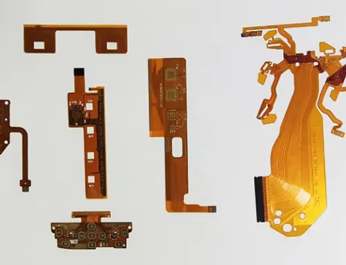
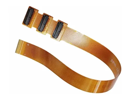
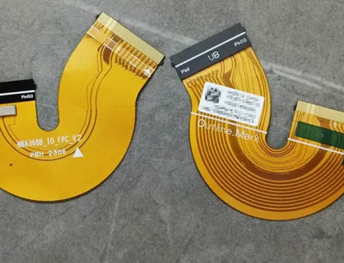
Flexible Printed Circuit Boards
Flexible Printed Circuit Boards (FlexPrintCircuit, abbreviated as “FPC”) are printed circuit boards manufactured using flexible substrates to form single-layer, double-layer, or multi-layer circuits.
They feature lightweight, thin profiles, compact dimensions, high density, exceptional stability, and flexible structures. Beyond static bending, they can withstand dynamic bending, curling, and folding.

Figure 1
Rigid Printed Circuit Board
Rigid Printed Circuit Boards (PCBs) are manufactured from non-deformable rigid substrate materials and remain flat during use. They offer high strength, minimal warping, and secure surface-mount component placement.
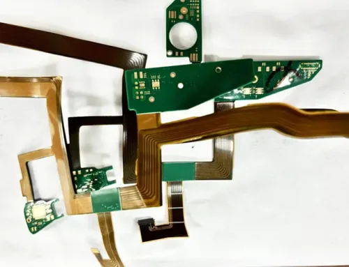
Rigid-Flex Boards
Rigid-flex boards are specialized flexible printed circuit boards formed by selectively laminating rigid and flexible substrates together.
They feature a compact structure with electrical connections via plated-through holes. These boards offer high density, fine traces, small apertures, compact size, light weight, and high reliability, maintaining stable performance under vibration, shock, and humid conditions.
Flexible and capable of 3D mounting, it maximizes installation space utilization and is widely adopted in portable digital devices like mobile phones, digital cameras, and camcorders.
Rigid-flex boards are increasingly used in packaging reduction applications, particularly in consumer electronics.
PCB Material Overview
Conductive Medium: Copper (CU)
— Copper Foil: Rolled Annealed (RA), Electrolytic (ED), High Tensile Electrolytic (HTE)
— Thickness: 1/4OZ, 1/3OZ, 1/2OZ, 1OZ, 2OZ (common specifications)
—OZ (Ounce): Copper foil thickness unit; 1OZ = 1.4 mil
Insulation Layer: Polyimide (PI), Polyester (PET), Polyethylene Naphthalate (PEN)
—Most commonly used: Polyimide (abbreviated as “PI”)
——PI thicknesses: 1/2 mil, 1 mil, 2 mil (these are the most common thicknesses)
——1 mil = 0.0254mm = 25.4μm = 1/1000 inch
Adhesive: Epoxy-based, Acrylic-based.
——Epoxy-based is more commonly used; thickness varies by manufacturer
Copper-clad laminates (CCL):
— Single-sided CCL: 3LCCL (with adhesive), 2LCCL (without adhesive). See illustrations below.
— Double-sided CCL: 3LCCL (with adhesive), 2LCCL (without adhesive). See illustrations below.

Figure 2: 3L single-sided copper-clad laminate and 2L single-sided copper-clad laminate
Coverlay (CVL):
Composed of an insulating layer and adhesive, applied over conductors to provide protection and insulation. Specific laminate structure as follows:

Figure 3

Figure 4
Supporting Materials:
1. Stiffener: Includes FR4, PI, SUS…
2. Conductive Silver Foil: Electromagnetic Shielding Film
——Type: SF-PC6000 (Black, 16μm)
——Advantages: Ultra-thin, excellent sliding and flex properties, high-temperature reflow soldering compatibility, superior dimensional stability.
Commonly used is SF-PC6000, with the following laminate structure:

Figure 5
Rigid-Flex Laminate Structure Display

Fig 6 Rigid-Flex Stacked Display
Flex PCB Manufacturing Process

Figure 7: Double-sided FPC board manufacturing process flowchart
Material Cutting: Shearing

Figure 8 Material Cutting: Shearing
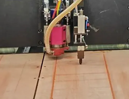
CNC Drilling

Fig 9 CNC Drilling
Through-Hole Plating
")
Figure 10: Plating Through Hole(1)
")
Figure 11 Plating Through Hole(2)
")
Fig 12: Plating Through Hole(3)
")
Figure 13: Plating Through Hole(4)
DES Process (Five Steps)
(1) Film Application (Dry Film Application)

Figure 14: Applying film and cutting film
(2) Exposure
Processing Environment: Yellow Light
Processing Purpose:
UV light exposure and mask alignment cause photopolymerization between the transparent areas of the film and the dry film.
Areas where the film is brown (opaque to UV light) prevent UV penetration, inhibiting photopolymerization between the film and corresponding dry film.

Figure 15: exposure
(3) Development
Process Solution: Na₂CO₃ (or K₂CO₃) weak alkaline solution
Process Purpose: The weak alkaline solution removes the unpolymerized portions of the dry film.

Figure 16: development
(4) Etching
Process Solution: Acidic Oxygenated Water: HCl + H₂O₂
Process Purpose: Use the chemical solution to etch away the exposed copper after development, thereby forming the pattern transfer.

Figure 17: Etching
(5) Stripping
Process Solution: Strong Alkaline NaOH Solution

Figure 18: Stripping
AOI
Primary Equipment: AOI, VRS System
Copper foil with formed circuits undergoes AOI scanning to detect circuit defects. Standard circuit image data is stored in the AOI host.
A CCD optical imaging head scans circuit information from the copper foil into the host for comparison with stored standard data. Abnormalities trigger location-coded defect records transmitted to the VRS host.
The VRS system magnifies the copper foil 300 times and sequentially displays the pre-recorded defect locations.
Operators assess whether each is a genuine defect. Genuine defects are marked with a water-based pen at the defect location to facilitate subsequent defect classification, statistical reporting, and repair by follow-up personnel. Operators use a 150x magnifying glass for assessment.
Defect types are categorized and statistically compiled into a quality report, which is fed back to the preceding process for timely implementation of improvement measures.
Due to the low defect rate and cost of single-sided boards, making AOI inspection impractical, manual visual inspection is employed.
False Attachment
Functions of Protective Film:
1) Insulation and solder resistance;
2) Circuit protection;
3) Enhancing flexible circuit bendability.

Figure 19: False Attachment
Hot Pressing
Process Conditions: High temperature and pressure
Surface Treatment
After hot pressing, exposed copper foil areas require surface treatment. Methods are determined based on customer specifications.

Figure 20: Surface Treatment
Screen Printing
Primary Equipment: Screen printer, oven, UV dryer. Screen printing equipment transfers ink onto the product using the screen printing principle. Primarily prints product batch numbers, production cycles, text, black masking, simple circuits, etc.
Positioning pins align the product with the screen. A squeegee applies pressure to force ink onto the product. The screen is open only in areas with text or patterns; areas without text or patterns are blocked by photosensitive emulsion, preventing ink from passing through.
After printing, products enter an oven for curing, bonding the printed text/pattern layer firmly to the surface.
Special requirements like adding partial traces (e.g., single-sided boards with extra traces for dual-layer functionality) or masking layers on dual-layer boards must be achieved through printing. UV-curable inks require UV dryers for curing.
Common defects: print skips, contamination, gaps, raised areas, peeling.
Testing (O/S Inspection)
Functional full inspection of PCBs using test fixtures + test software.
Punching
Corresponding contour dies: knife-edge die, laser cutting, etching die, simple steel die, steel die.
Processing & Assembly
Processing & assembly involves assembling components per customer requirements. Examples of supplier-requested assemblies include:
A. Stainless steel reinforcement
B. Beryllium copper/phosphor bronze/nickel-plated steel reinforcement
C. FR4 reinforcement
D. PI reinforcement
Inspection
Inspection items: Appearance, dimensions, reliability
Testing tools: 2D measuring system, micrometer, caliper, magnifying glass, solder pot, tensile tester.
Packaging
Packaging Methods:
- Plastic bag + cardboard
- Low-adhesion packaging material
- Standard vacuum box
- Dedicated vacuum box (anti-static grade)
Double-sided PCB Manufacturing Flowchart

Figure 21: Double-sided PCB board manufacturing process flowchart
Rigid-Flex PCB Manufacturing Flowchart

Figure 22: Rigid-Flex PCB Manufacturing Flowchart
PCB Case Study
I. Design Solution
Solution Description:
• The new COF solution integrates the reinforcement and chip bonding area onto a single steel substrate, as shown in the FPC schematic.
• Primary Applications:
1. Minimizes sensor contact with uneven PCB surfaces by directly bonding the sensor to the flat steel substrate
to maintain perpendicularity between the sensor and optical lens axes, reducing blurring defects.
2. For ≤0.3mm applications, the new COF offers superior flatness compared to rigid-flex boards, achieving lower module height while maintaining flatness.
3. Direct sensor-to-steel contact enhances thermal conductivity.

Figure 23: FPC diagram
Design Solution
1) P8V12G-621-00 PCB (Structural diagram below:)
PCB design thickness: 0.3mm; Steel plate stud height: 0.02mm.

Figure 24: P8V12G-621-00 Circuit Board Structure Diagram
2) P8V12G-621-00 PCB (Routing diagram below)

Figure 25 P8V12G-621-00 PCB Routing diagram
3) P8V12G-621-00 PCB (stackup diagram as follows)

Figure 26 P8V12G-621-00 PCB stackup diagram
4) PCB Design Constraint Assessment:
1. Purple boxes indicate steel plate support areas.
2. Support areas distributed diagonally relative to SENSOR;
3. Minimum support window size 0.5*0.5mm; larger areas improve flatness;
4. Module head dimensions ≥8.5*8.5mm;
5. Sensor pin count ≤80;
6. MIPI 2-lane output facilitates routing compared to 4-lane output;
7. MIPI placement near the connector end improves routing (e.g., pads beneath MIPI routing in the right diagram);

Figure 27 Circuit board design diagram
Comparative Analysis of Advantages and Disadvantages

Figure 28: Comparative Analysis of Advantages and Disadvantages
Flatness Data Comparison:
Flatness Comparison Across P8V12G Variants:

Figure 29: Comparison of flatness under different types of P8V12G
Flatness Deformation Comparison Before/After Reflow Across P8V12G Variants:

Figure 30: Comparison of flatness deformation before and after reflow of P8V12G
Conclusion
In summary, the technology encompasses a wide spectrum of structures, materials, and Flex PCB manufacturing processes tailored to meet increasingly stringent requirements in size, reliability, and performance.
Flexible, rigid, and rigid-flex PCBs each provide distinct advantages, supported by optimized material selections such as copper foils, polyimide substrates, coverlays, and reinforcing structures.
Through controlled processes—including drilling, plating, imaging, etching, lamination, surface treatment, and inspection—manufacturers achieve high-density interconnections with consistent quality.
The presented rigid-flex COF case study further demonstrates how innovative structural integration and material design can significantly improve flatness, thermal performance, and module miniaturization.
Together, these concepts illustrate how modern PCB engineering enables advanced electronic products across consumer, industrial, and high-precision applications.