What is the Multilayer flex PCB fabrication process?


As electronic systems continue to shrink while delivering greater functionality, multilayer flex PCBs have become a foundational technology for high-density, space-constrained, and dynamically moving applications.
Unlike traditional rigid boards, multilayer flexible printed circuits allow engineers to route complex interconnections across multiple conductive layers while maintaining mechanical flexibility—an increasingly non-negotiable requirement in modern product design.
A multilayer flex PCB is defined by the integration of three or more copper conductor layers laminated onto flexible dielectric substrates, typically polyimide-based materials. This structure enables high wiring density within an ultra-thin form factor, while still tolerating repeated bending, folding, or vibration.
These characteristics make multilayer flex PCBs indispensable in applications where miniaturization, signal integrity, and mechanical compliance must coexist. Smartphones and wearables rely on them to interconnect densely packed components;
automotive electronics use them in constrained, vibration-prone environments; medical devices demand flexibility without sacrificing reliability;
and lithium battery systems depend on multilayer flex circuits to manage sensing, balancing, and power routing within tight packaging envelopes.
What distinguishes this article from most existing content is its focus not only on definitions, but on manufacturing processes, material selection, stack-up design, and manufacturability considerations—the aspects that ultimately determine yield, reliability, and cost in real-world production.
What Is a Multilayer Flex PCB? (Clear Technical Definition)
A multilayer flex PCB is a flexible printed circuit consisting of three or more conductive copper layers, separated by flexible dielectric films and bonded through lamination. These layers are electrically interconnected using plated through-holes (PTHs), microvias, or laser-drilled vias, depending on density requirements.
The core materials typically consist of Flexible Copper-Clad Laminates (FCCL), most commonly using polyimide (PI) or, in lower-cost and lower-temperature applications, polyethylene terephthalate (PET).
Copper thickness usually ranges from 9 µm to 35 µm per layer, with overall circuit thickness often below 0.3 mm, even for four-layer designs.
It is important to clearly distinguish multilayer flex PCBs from similar technologies:
| PCB Type | Mechanical Behavior | Typical Layer Count | Key Use Case |
|---|---|---|---|
| Single-layer flex | Fully flexible | 1 | Simple signal routing |
| Double-layer flex | Flexible | 2 | Moderate routing density |
| Multilayer flex | Fully flexible | ≥3 | High-density, bending applications |
| Rigid-flex PCB | Rigid + flexible zones | ≥2 flex + rigid layers | Structural + flex integration |
A multilayer flex PCB remains flexible throughout its entire structure, whereas a rigid-flex PCB incorporates rigid FR4 sections for component mounting and mechanical stability.
In practice, multilayer flex is preferred when the design requires continuous bending, ultra-thin profiles, or weight reduction. Rigid-flex becomes advantageous when high component density, heavy connectors, or mechanical reinforcement are required.

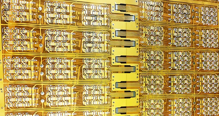
Flex PCB
Typical Multilayer Flex PCB Stack-Up Structures
The stack-up design of a multilayer flex PCB directly determines its electrical performance, flexibility, thickness, and long-term reliability. Two fundamental stack-up philosophies dominate industrial production: adhesive-based and adhesive-free (adhesiveless) constructions.
In adhesive-based stack-ups, individual FCCL layers are bonded using acrylic or epoxy adhesives. This approach offers cost advantages and easier processing but introduces additional thickness and potential reliability risks under thermal cycling.
Adhesive-free stack-ups eliminate bonding adhesives by directly casting or laminating copper onto polyimide films. These structures are thinner, more dimensionally stable, and better suited for high-temperature or dynamic bending environments.
A simplified comparison is shown below:
| Stack-Up Type | Typical Thickness | Flex Fatigue Life | Thermal Stability |
|---|---|---|---|
| Adhesive-based | Higher | Moderate | Limited by adhesive Tg |
| Adhesive-free | Lower | High | Excellent (PI-controlled) |
Key structural elements include the coverlay, which replaces solder mask in flex circuits and provides mechanical protection; bonding layers or low-flow prepregs, which control resin spread during lamination; and copper foil selection, which affects both electrical conductivity and mechanical endurance.
Poor stack-up design can lead to copper cracking, delamination, or impedance instability, especially in multilayer constructions where internal stresses accumulate.
Materials Used in Multilayer Flex PCB Fabrication
Flexible Copper-Clad Laminates (FCCL)
FCCL is the foundational material of multilayer flex PCBs, consisting of copper foil laminated onto a flexible dielectric film.
Polyimide (PI) is the industry standard due to its high glass transition temperature (>300°C), excellent chemical resistance, and low coefficient of thermal expansion. PET-based FCCL is sometimes used for consumer-grade electronics but is limited by lower thermal endurance.
| Property | PI-Based FCCL | PET-Based FCCL |
|---|---|---|
| Max operating temperature | ~200–260°C | ~120–150°C |
| Dimensional stability | Excellent | Moderate |
| Cost | Higher | Lower |
Adhesive-free FCCL further improves dimensional stability and reduces z-axis expansion, making it the preferred choice for multilayer flex designs with fine-pitch vias.
Copper Foil Types
Copper foil selection is critical in multilayer flex PCBs, particularly when dynamic bending is involved.
Rolled Annealed (RA) copper exhibits elongated grain structure, allowing it to withstand millions of flex cycles without cracking. Electrodeposited (ED) copper, while more economical, has a columnar grain structure that is less tolerant of repeated bending.
| Copper Type | Flex Performance | Cost | Typical Use |
|---|---|---|---|
| RA copper | Excellent | Higher | Dynamic flex zones |
| ED copper | Moderate | Lower | Static or limited-flex areas |
In multilayer constructions, RA copper is strongly recommended for inner layers that experience mechanical stress.
Stiffeners and Reinforcement Options
Although multilayer flex PCBs are inherently flexible, stiffeners are often introduced locally to support connectors, components, or solder joints. Common stiffener materials include FR4 for cost efficiency, polyimide for thermal compatibility, and stainless steel for maximum mechanical strength in ultra-thin designs.
Stiffeners are not structural necessities but functional reinforcements, carefully placed to balance flexibility and mechanical integrity.
Overview of the Multilayer Flex PCB Fabrication Process
Manufacturing a multilayer flex PCB is significantly more complex than producing a rigid board, primarily due to material sensitivity and tight process tolerances.
The end-to-end process begins with FCCL preparation and inner-layer circuit imaging, followed by controlled lamination to build the multilayer structure. Laser drilling or mechanical drilling creates vias, which are then copper-plated to establish interlayer connectivity.
Subsequent steps include outer-layer patterning, coverlay lamination, surface finishing, and electrical testing.
Unlike rigid PCBs, multilayer flex fabrication requires precise control of lamination pressure, temperature, and resin flow. Excessive stress or misalignment can permanently distort the flexible substrate, leading to registration errors or reduced flex life.
As layer count increases, the margin for error narrows. This is why multilayer flex PCB production is often limited to manufacturers with specialized equipment and process expertise, especially for applications involving fine-line routing, impedance control, or dynamic motion.
Step-by-Step Multilayer Flex PCB Fabrication Process
The fabrication of multilayer flex PCBs demands far tighter control than rigid or single-layer flexible circuits. Each step influences not only electrical performance, but also bend life, dimensional accuracy, and long-term reliability.
The following process flow reflects industry-proven manufacturing practice for high-density multilayer flex circuits.

Multilayer Flex PCB Fabrication Process
Step 1: Flexible Inner Layer Circuit Fabrication
The process begins with the fabrication of individual inner-layer circuits on FCCL material. Circuit patterns are typically defined using photoimaging and chemical etching, although laser direct structuring is increasingly adopted for ultra-fine features.
Fine-line flex circuits commonly operate in the 50–75 μm line/space range, with advanced designs pushing below 40 μm. Unlike rigid boards, flexible substrates are prone to dimensional movement during imaging and etching. As a result, tension control, panel support, and exposure compensation are critical to prevent line width distortion.
Copper thickness selection at this stage also has mechanical implications. Thinner copper improves bend performance but reduces current-carrying capacity, requiring careful trade-offs during inner-layer design.
Step 2: Coverlay Application and Opening Control
After inner-layer patterning, coverlay is applied to protect copper traces and provide insulation. Coverlay typically consists of polyimide film coated with adhesive, laminated under heat and pressure.
Two coverlay strategies are commonly used. Full-cover coverlay protects the entire circuit surface and is preferred for dynamic flex regions, while windowed coverlay selectively exposes pads for soldering or bonding. Opening definition is achieved through laser cutting or mechanical punching, with positional accuracy often held within ±50 μm for fine-pitch components.
Coverlay thickness and opening geometry directly affect both bendability and solder joint reliability. Excessive adhesive flow into pad openings can compromise solderability, while overly rigid coverlay structures can concentrate stress at bend transition zones.
Step 3: Layer Alignment and Lay-Up Design
Multilayer flex PCBs are laminated as a stack of precisely aligned layers. Prior to lamination, individual layers are arranged according to a defined lay-up design, often using multi-panel configurations such as 4-in-1 or 6-in-1 arrays to improve material utilization and processing efficiency.
Registration accuracy is one of the most critical parameters at this stage. Typical alignment tolerances for multilayer flex circuits are ±25–40 μm, significantly tighter than many rigid PCB applications. Optical alignment systems and precision tooling holes are commonly employed to achieve this level of accuracy.
Improper alignment can lead to via misregistration, annular ring breakout, or impedance variation—defects that are difficult or impossible to correct later in the process.
Step 4: Lamination of Multilayer Flex Stack-Up
Lamination transforms individual layers into a unified multilayer structure. Vacuum lamination is widely used for multilayer flex PCBs, as it minimizes air entrapment and ensures uniform adhesive flow across the panel.
Low-flow adhesives or specialized prepregs are selected to prevent excessive resin squeeze-out, which can stiffen flexible regions and reduce bend life. Pressure balancing plates and filler materials are often added to ensure uniform pressure distribution during lamination.
Pre-baking of materials prior to lamination is a critical but sometimes overlooked step. Removing absorbed moisture from polyimide and adhesives reduces the risk of delamination, void formation, and blistering, particularly during subsequent high-temperature processes.
Step 5: Drilling, Via Formation, and Hole Preparation
Once laminated, interlayer connections are formed through drilling. Mechanical drilling is typically used for larger vias, while laser drilling is preferred for microvias and high-density interconnections.
Flexible substrates present unique challenges during drilling due to their elasticity. Improper backing materials or drill parameters can cause hole deformation or smear. To address this, plasma desmear and controlled etchback processes are used to clean hole walls and expose clean copper surfaces for metallization.
Via reliability is especially critical in multilayer flex PCBs, as vias often experience mechanical strain during bending. Aspect ratio control and smooth hole wall quality are essential to prevent early fatigue failure.
Step 6: Metallization and Copper Plating
Metallization establishes electrical continuity between layers. The process typically involves electroless copper deposition followed by electrolytic copper plating to build up the required wall thickness.
In flex circuits, plating thickness must be carefully controlled. Excessive copper increases stiffness and stress concentration, while insufficient plating compromises via reliability. Typical through-hole copper thickness for flex applications ranges from 18 to 25 μm, depending on bend requirements.
Uniform plating distribution is more difficult to achieve on flexible panels, making bath chemistry control and panel handling particularly important.
Step 7: Outer Layer Imaging and Etching
Outer-layer circuitry is defined using photoimaging and etching, similar to inner layers but with additional challenges. Flexible panels can stretch or wrinkle during processing, making fixture support and tension management critical to maintain pattern accuracy.
Fine-pitch outer-layer features must align precisely with underlying vias and pads. Any dimensional instability at this stage can result in open circuits or reduced solder joint reliability.
Step 8: Surface Finish Application
Surface finish selection directly affects solderability, corrosion resistance, and long-term performance. Common finishes for multilayer flex PCBs include ENIG, OSP, immersion silver, immersion tin, and hard gold.
ENIG is widely used for fine-pitch SMT and offers good surface planarity, while OSP is favored for cost-sensitive applications with controlled assembly processes. Hard gold is typically reserved for edge contacts or wear-resistant interfaces.
The operating environment—temperature, humidity, mechanical wear—should always guide surface finish selection.
Step 9: Profiling, Cutting, and Final Forming
The final step involves separating individual circuits from the production panel. Laser cutting is increasingly preferred for multilayer flex PCBs due to its precision and minimal mechanical stress. Mechanical routing may still be used for simpler geometries but requires careful control to avoid edge cracking.
Edge quality is particularly important in flex circuits, as micro-cracks can propagate under repeated bending. Final forming operations, such as folding or pre-bending, are sometimes performed to meet assembly requirements.
Assembly Considerations for Multilayer Flex PCBs
Assembly introduces a new set of challenges unique to flexible substrates. Unlike rigid boards, multilayer flex PCBs lack inherent structural stiffness, making support during SMT processes essential.
Temporary carriers or fixtures are commonly used to maintain flatness during solder paste printing, component placement, and reflow. These carriers must accommodate thermal expansion without inducing stress or warpage.
Dimensional movement during reflow can affect component alignment, particularly for fine-pitch packages. Post-assembly inspection often relies more heavily on AOI and X-ray inspection, as flex circuits may not remain perfectly planar after assembly.
Proper assembly process design is critical to prevent latent defects that only appear after the product enters service.
Key Manufacturing Challenges and How to Mitigate Them
Despite technological advances, multilayer flex PCB manufacturing presents persistent challenges.
Dimensional stability at elevated temperatures remains a major concern, particularly during lamination and reflow. This is mitigated through material selection (adhesive-free PI systems), pre-baking, and optimized process profiles.
Adhesive overflow can unintentionally stiffen flex regions. Using low-flow adhesives and carefully designed lamination pressure profiles helps preserve intended flexibility.
Via cracking under dynamic bending is one of the most common long-term failure modes. This risk is reduced by controlling via placement, minimizing copper thickness transitions, and avoiding vias in high-strain bend areas whenever possible.
Finally, yield loss in high-layer-count flex boards is often driven by cumulative tolerances and material variability. Robust DFM rules, early supplier involvement, and tight process monitoring are essential to maintaining acceptable yields as complexity increases.
Design Tips to Improve Multilayer Flex PCB Manufacturability
Successful multilayer flex PCB projects are determined as much by design discipline as by manufacturing capability. Designs that ignore flex-specific constraints often suffer from low yield, poor reliability, or unnecessary cost escalation.
From a routing perspective, trace width and spacing should be selected not only based on electrical requirements, but also on mechanical durability. In dynamic bending regions, wider traces with smooth, gradual transitions perform better than narrow, high-aspect-ratio conductors.
As a general industry practice, line/space below 50 μm should be limited to static flex zones, unless advanced materials and RA copper are used.
Bend area design is one of the most critical aspects of multilayer flex PCB manufacturability. Copper traces should be routed perpendicular to the bend axis, avoiding sharp corners and sudden width changes.
Staggering traces across layers instead of stacking them directly on top of each other significantly reduces strain concentration during flexing. Neutral axis design—placing critical signal layers near the mechanical center of the stack-up—can dramatically extend flex life.
Via placement requires particular caution. Vias should be kept out of dynamic bend regions whenever possible. When unavoidable, microvias with reduced copper thickness and generous annular rings perform better than traditional plated through-holes.
Blind and buried vias are often preferred in multilayer flex designs to reduce overall stress and thickness.
Copper balancing strategies also play a key role. Uneven copper distribution across layers can cause lamination distortion and unpredictable bending behavior. Balanced copper planes or patterned copper thieving help maintain symmetry, improving both manufacturability and dimensional stability.
Material selection should always align with the mechanical and thermal demands of the application. Adhesive-free PI-based FCCL combined with RA copper offers the best long-term reliability for dynamic flexing, while adhesive-based systems may be acceptable for static or cost-sensitive designs.
Multilayer Flex PCB Capabilities and Typical Specifications
Understanding typical manufacturing capabilities helps engineers design within realistic and cost-effective boundaries. While exact limits vary by supplier, the following ranges reflect mainstream industrial production capability rather than laboratory extremes.
| Parameter | Typical Capability Range |
|---|---|
| Layer count | 3 to 10 layers (up to 12 for advanced suppliers) |
| Finished thickness | 0.15 mm – 0.40 mm |
| Minimum line/space | 40/40 μm (50/50 μm standard) |
| Copper thickness | 9, 12, 18, 35 μm |
| Via diameter (laser) | ≥75 μm |
| Panel size | ~250 × 350 mm (varies by equipment) |
As layer count increases, tolerances tighten and yields naturally decrease. For this reason, many high-reliability designs prioritize optimized routing and stack-up efficiency over simply adding layers.
It is also important to note that not all manufacturers can support the full range of these specifications simultaneously. For example, ultra-fine line/space combined with high layer count and large panel sizes significantly increases process complexity.
How to Choose the Right Multilayer Flex PCB Manufacturer
Selecting a multilayer flex PCB manufacturer should be treated as an engineering partnership decision, not merely a purchasing exercise.
Engineering support capability is often the most telling indicator of a supplier’s competence. Manufacturers with dedicated flex PCB engineering teams can provide early DFM feedback, stack-up optimization, and material recommendations that prevent costly redesigns later.
Material sourcing strategy also matters. Suppliers with in-house FCCL processing or long-term material partnerships tend to offer better consistency, traceability, and lead-time stability than those relying entirely on spot-market sourcing.
Process certifications provide another layer of assurance. IPC standards such as IPC-6013 (flexible printed boards), along with ISO 9001, IATF 16949 for automotive, and UL recognition, indicate mature process control. For medical or aerospace applications, demonstrated experience with high-reliability qualification is often more important than price.
Finally, past experience with similar applications—whether in consumer electronics, automotive electronics, or medical devices—can significantly reduce technical and schedule risk.
Conclusion: When Multilayer Flex PCBs Are the Right Choice
Multilayer flex PCBs represent one of the most technically demanding segments of the PCB industry, combining high-density electrical design with strict mechanical reliability requirements. Their fabrication requires specialized materials, precise process control, and close collaboration between design and manufacturing teams.
For OEMs and engineers, the decision to use multilayer flex should be driven by clear functional advantages: extreme space constraints, high interconnection density, weight reduction, or the need to survive repeated bending or vibration. When these benefits outweigh the added complexity and cost, multilayer flex PCBs offer performance levels that rigid or rigid-flex solutions cannot match.
The key takeaway is balance. Optimal multilayer flex PCB designs carefully trade off performance, reliability, and manufacturability—leveraging advanced materials and thoughtful stack-up design while staying within proven production capabilities.
When applied appropriately, multilayer flex PCBs are not just a packaging solution, but a critical enabler of next-generation electronic systems.
References
IPC-2223: Sectional Design Standard for Flexible Printed Boards
IPC-6013: Qualification and Performance Specification for Flexible Printed Boards
IPC-4101: Specification for Base Materials for Rigid and Multilayer Printed Boards
DuPont™ Kapton® Polyimide Film Technical Data Sheets
ASM Electronics Manufacturing Handbook, Flexible Circuit Technology Section
Altium Designer Technical Papers on Flex and Rigid-Flex PCB Design

