What Is a Flex PCB and How Does It Work?


Traditional rigid printed circuit boards have served the electronics industry for decades, but their inherent mechanical rigidity increasingly limits product design in modern applications.
Why Flex PCBs Matter in Modern Electronics
Rigid PCBs cannot tolerate bending, folding, or continuous motion, which forces designers to rely on connectors, cables, and mechanical allowances that increase size, weight, and assembly complexity. As electronic products evolve toward smaller form factors and higher functional density, these constraints become more pronounced.
The rapid growth of compact, lightweight, and movable electronics has driven demand for interconnection solutions that can conform to three-dimensional shapes and withstand mechanical stress.
Devices such as smartphones, wearable electronics, automotive camera modules, medical instruments, and industrial sensors all require electrical connections that move with the product rather than resist it. In these scenarios, flexible printed circuit boards provide a decisive advantage by replacing bulky wiring harnesses and rigid interconnects with thin, lightweight, and mechanically resilient circuitry.
Flex PCBs consistently outperform rigid designs in applications involving folding enclosures, dynamic hinges, vibration exposure, or space-constrained assemblies.
By enabling circuits to bend, twist, and integrate directly into mechanical structures, flex PCBs allow engineers to reduce part count, improve reliability, and achieve design geometries that are impossible with rigid boards alone.

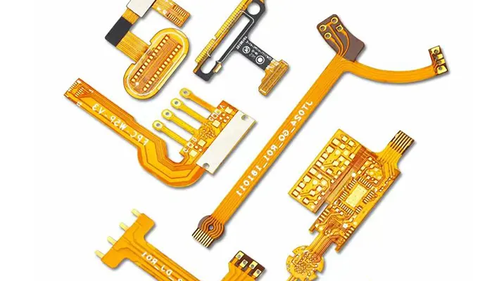
Flex pcb
What Is a Flex PCB? (Technical Definition)
A Flexible Printed Circuit Board, commonly referred to as a flex PCB or FPC, is an electrical interconnection circuit fabricated on a thin, flexible dielectric substrate—most often polyimide—that allows the circuit to bend, fold, or dynamically flex during use.
Unlike rigid PCBs, flex circuits are designed to endure mechanical deformation while maintaining electrical continuity and signal integrity.
The defining characteristics of a flex PCB include its thin profile, typically ranging from 25 µm to under 200 µm depending on layer count and construction, its ability to withstand repeated bending cycles, and its high mechanical endurance relative to its thickness.
Properly designed flex circuits can survive millions of bend cycles at controlled radii, far exceeding the durability of traditional wiring solutions.
In industry literature, the terms Flex PCB, FPC, and Flexible Circuit Board are used interchangeably, though “flexible printed circuit” is the formal terminology used in IPC standards such as IPC-2223 and IPC-6013.
The origins of flexible circuits date back to the early 1950s, when flexible wiring concepts were developed for aerospace and military applications in the United States.
One of the earliest documented uses of flexible circuitry was in missile guidance systems, where weight reduction and vibration resistance were critical.
Commercial adoption accelerated in the 1960s and 1970s with advances in polyimide materials, particularly following DuPont’s introduction of Kapton® polyimide film, which remains a cornerstone material in flex PCB manufacturing today.
Flex PCB vs. Other PCB Types
Flex PCB vs. Rigid PCB
The fundamental difference between flex and rigid PCBs lies in material selection and mechanical behavior. Rigid PCBs are typically constructed from glass-reinforced epoxy laminates such as FR-4, which provide stiffness and dimensional stability but cannot tolerate bending without fracture.
Flex PCBs, by contrast, use polymer dielectrics such as polyimide that combine high tensile strength with flexibility.
From an assembly and reliability perspective, flex PCBs often reduce the need for connectors and cables, which are common failure points in rigid-board-based designs.
Studies in automotive and industrial electronics have shown that eliminating connectors can improve system reliability by reducing contact resistance variation and vibration-induced failures.
Over the product lifecycle, flex PCBs also enable fewer interconnects, lower mass, and improved shock and vibration resistance.
Flex PCB vs. Rigid-Flex PCB
Rigid-flex PCBs represent a hybrid architecture that integrates rigid PCB sections with flexible interconnect regions into a single structure. Structurally, rigid-flex designs combine FR-4-based rigid layers and polyimide-based flex layers within a unified stack-up, eliminating the need for board-to-board connectors.
Pure flex PCBs are typically used as interconnects or cable replacements, while rigid-flex PCBs support component mounting on rigid sections alongside flexible routing. Rigid-flex designs are common in aerospace, medical, and high-reliability systems where space constraints and mechanical robustness justify higher manufacturing complexity.
From a cost perspective, flex PCBs are generally less expensive than rigid-flex designs due to simpler stack-ups and fewer lamination steps. However, rigid-flex PCBs can reduce total system cost by simplifying assembly and improving reliability, particularly in complex electromechanical products.
| Aspect | Flex PCB | Rigid PCB | Rigid-Flex PCB |
|---|---|---|---|
| Base Materials | Polyimide or other flexible polymer dielectrics | Glass-reinforced epoxy (FR-4) | Combination of FR-4 (rigid) and polyimide (flex) |
| Mechanical Behavior | Highly flexible; can bend, fold, and conform to shapes | Rigid and dimensionally stable; fractures if bent | Rigid sections for stability with flexible interconnect regions |
| Structural Role | Often used as interconnects or cable replacements | Primary structural circuit board | Integrated structure combining rigid mounting areas and flexible routing |
| Component Mounting | Limited or none (depends on design) | Full component population | Components mounted on rigid sections |
| Connectors & Cables | Often eliminates connectors and cables | Requires connectors for board-to-board connections | Eliminates board-to-board connectors within the system |
| Reliability | High reliability due to fewer interconnects and reduced vibration sensitivity | Connector-related failures more common | Very high reliability; reduced contact resistance and vibration failures |
| Shock & Vibration Resistance | Excellent | Moderate | Excellent |
| Weight & Space Efficiency | Very lightweight and space-saving | Heavier and bulkier | Optimized for compact, high-density systems |
| Manufacturing Complexity | Moderate | Low | High (complex stack-up and lamination) |
| Cost (PCB Level) | Lower than rigid-flex | Lowest | Highest |
| Cost (System Level) | Can reduce cost by simplifying assembly | Higher due to connectors and wiring | Often reduces total system cost despite higher PCB price |
| Typical Applications | Consumer electronics, cable replacement, dynamic interconnects | General electronics, industrial controls | Aerospace, medical devices, automotive, high-reliability systems |
Types of Flex PCBs
Single-sided flex PCBs consist of one conductive copper layer bonded to a flexible dielectric substrate and protected by a coverlay. Their simplicity provides maximum flexibility and excellent fatigue resistance, making them ideal for dynamic bending applications such as hinges, sliders, and moving sensor connections.
Double-sided flex PCBs incorporate two copper layers interconnected through plated through-holes or microvias. This structure increases routing density and allows for basic grounding and impedance control, but reduces flexibility compared to single-sided designs.
Careful bend-zone definition is required to prevent via-related fatigue failures.
Multilayer flex PCBs include three or more conductive layers separated by flexible dielectrics.
These designs support high signal density, controlled impedance, and power distribution but are generally intended for static or limited-flex applications due to increased thickness and reduced bend tolerance.
Rigid-flex PCBs integrate rigid and flexible sections into a single assembly, combining the electrical performance of rigid boards with the mechanical adaptability of flex circuits.
They are widely used in aerospace avionics, medical imaging systems, and advanced consumer electronics, where reliability and space efficiency are paramount.
Flex PCB Stack-Up and Construction Explained
A typical flex PCB stack-up consists of a flexible dielectric substrate, copper conductors, optional adhesive layers, and a polyimide coverlay for protection. The exact arrangement and thickness of these layers define the mechanical and electrical behavior of the circuit.
Even small changes in stack-up can significantly affect bend radius, fatigue life, and signal performance.
Stack-up design directly influences flexibility and reliability by determining where copper layers sit relative to the neutral axis during bending. Thinner constructions with copper positioned near the neutral axis experience lower strain and longer flex life.
Conversely, excessive thickness or poorly placed copper layers increase stress concentration and accelerate failure.
Flex PCB stack-ups are also categorized based on whether they are intended for static or dynamic flexing. Static flex designs tolerate bending during installation but remain fixed during operation, allowing for thicker constructions and higher layer counts.
Dynamic flex designs must withstand continuous or repeated bending, requiring ultra-thin dielectrics, rolled annealed copper, and optimized layer placement to achieve long-term durability.
Materials Used in Flex PCBs
Material selection is the foundation of flex PCB performance, directly influencing mechanical endurance, electrical stability, thermal reliability, and long-term durability.
Unlike rigid PCBs, where material choices are relatively standardized, flexible circuits rely on a carefully balanced combination of polymer dielectrics, copper foils, protective layers, and local reinforcements to achieve the required flexibility without sacrificing reliability.
Base Dielectric Materials
Polyimide (PI) is the dominant base dielectric material used in flex PCBs and has become the industry standard due to its exceptional thermal and mechanical properties.
Typical polyimide films used in flex circuits range from 12.5 µm to 50 µm in thickness and maintain mechanical integrity at continuous operating temperatures of 150–200 °C, with short-term exposure limits exceeding 300 °C.
PI exhibits low thermal expansion, high tensile strength, and excellent chemical resistance, making it suitable for demanding applications such as automotive electronics, aerospace systems, and medical devices.
Alternative dielectric materials such as polyethylene terephthalate (PET) and polyethylene naphthalate (PEN) are occasionally used in cost-sensitive consumer electronics.
While these materials offer acceptable flexibility and lower raw material cost, their thermal stability is significantly inferior to polyimide. PET, for example, typically has a maximum operating temperature below 120 °C, which limits its suitability for lead-free soldering processes and high-reliability environments.
As a result, PET- and PEN-based flex circuits are generally confined to low-temperature, static-flex applications with limited service life expectations.
| Material | Thermal Performance | Mechanical Properties | Cost Level | Typical Use |
|---|---|---|---|---|
| Polyimide (PI) | 150–200 °C continuous, >300 °C short-term | High tensile strength, low CTE, excellent chemical resistance | High | Automotive, aerospace, medical, high-reliability flex PCBs |
| PET / PEN | <120 °C max operating temperature | Acceptable flexibility, limited durability | Low | Cost-sensitive, low-temperature, static-flex applications |
Copper Foil
Copper foil selection plays a critical role in determining flex life and fatigue resistance. Rolled annealed (RA) copper is specifically engineered for flexible circuits and exhibits a grain structure aligned in the rolling direction, which allows the copper to elongate under bending stress.
RA copper is commonly available in thicknesses from 9 µm to 35 µm and is capable of surviving hundreds of thousands to millions of dynamic bending cycles when properly designed.
Electro-deposited (ED) copper, by contrast, has a columnar grain structure that is more prone to crack initiation under repeated flexing.
Although ED copper is widely used in rigid PCBs due to its lower cost and ease of processing, its fatigue performance in flex applications is significantly inferior. For this reason, ED copper is typically restricted to static-flex or non-bending areas of flex or rigid-flex designs.
| Copper Type | Grain Structure | Flex Life | Thickness Range | Recommended Areas |
|---|---|---|---|---|
| Rolled Annealed (RA) | Aligned rolling grain | Very high (dynamic bending capable) | 9–35 µm | Dynamic flex zones |
| Electro-Deposited (ED) | Columnar grain | Low under repeated bending | Common rigid PCB ranges | Static-flex or non-bending areas |
Coverlay vs. Solder Mask
In flexible circuits, coverlay replaces the traditional liquid photoimageable solder mask used on rigid PCBs. Coverlay consists of a thin polyimide film coated with adhesive and laminated over the copper circuitry, with openings mechanically or laser-defined for pads and component interfaces.
This construction provides superior mechanical protection, insulation, and strain relief, especially in bending zones.
Solder mask, while common on rigid sections of rigid-flex boards, lacks the flexibility and adhesion strength required for dynamic flex applications.
Coverlay also offers improved resistance to cracking, delamination, and moisture ingress, making it essential for high-reliability flex designs.
| Protection Method | Flexibility | Mechanical Protection | Reliability in Bending | Typical Use |
|---|---|---|---|---|
| Coverlay | Excellent | High strain relief and insulation | Very high | Dynamic flex areas |
| Solder Mask | Poor | Limited | Low | Rigid sections of rigid-flex PCBs |
Adhesive vs. Adhesiveless Construction
Adhesive-based flex circuits use a separate adhesive layer to bond copper foil to the polyimide substrate. This construction is cost-effective and widely available but introduces additional thickness and potential reliability concerns.
Adhesive layers can degrade over time under thermal cycling, absorb moisture, and contribute to delamination in harsh environments.
Adhesiveless construction eliminates the adhesive layer by directly bonding copper to polyimide through casting or sputtering processes. The resulting structure is thinner, more dimensionally stable, and thermally robust.
Adhesiveless flex circuits exhibit superior flex life, improved high-temperature performance, and lower dielectric loss, making them the preferred choice for dynamic bending, high-speed signal transmission, and long-life applications.
| Construction Type | Structure | Thickness | Thermal Reliability | Flex Performance |
|---|---|---|---|---|
| Adhesive-Based | Copper + adhesive + PI | Thicker | Moderate | Limited flex life |
| Adhesiveless | Direct copper-to-PI bond | Thinner | High | Superior dynamic flex life |
Stiffeners
Designers locally apply stiffeners to provide mechanical support in areas that require component mounting, connector insertion, or repeated mechanical loading. They commonly use FR4 for general-purpose reinforcement, stainless steel for thin yet rigid support, and aluminum when thermal dissipation is also necessary.
Designers typically place stiffeners under connectors, soldered components, or interface regions to prevent excessive flexing and solder joint fatigue. They carefully manage placement to avoid creating stress concentration points at the transition between rigid and flexible regions.
| Stiffener Material | Key Function | Advantage | Common Placement |
|---|---|---|---|
| FR4 | General mechanical support | Cost-effective, widely used | Under components, connectors |
| Stainless Steel | High rigidity, thin profile | Strong with minimal thickness | Connector interfaces |
| Aluminum | Mechanical support + heat dissipation | Thermal management | Power or heat-sensitive areas |
Surface Finishes
Surface finish selection affects solderability, corrosion resistance, and long-term reliability. Manufacturers widely apply electroless nickel immersion gold (ENIG) for its flat surface, excellent solderability, and compatibility with fine-pitch components.
Immersion silver offers superior electrical performance for high-frequency signals but requires controlled handling to prevent tarnishing.
Organic solderability preservatives (OSP) provide a cost-effective and lightweight option but have limited shelf life and durability. Designers occasionally use immersion tin but must carefully control the process to avoid whisker formation.
| Surface Finish | Key Benefit | Reliability Consideration | Typical Application |
|---|---|---|---|
| ENIG | Flat surface, excellent solderability | High long-term stability | Fine-pitch, high-reliability designs |
| Immersion Silver | Excellent conductivity | Tarnishing risk | High-frequency circuits |
| OSP | Low cost, lightweight | Short shelf life | Cost-sensitive products |
| Immersion Tin | Good solderability | Whisker risk if uncontrolled | Selective applications |
Flex PCB Thickness and Mechanical Flexibility
Flex PCB thickness is a primary determinant of mechanical flexibility and allowable bend radius. Single-layer flex circuits commonly range from 50 µm to 150 µm in total thickness, while multilayer flex and rigid-flex constructions can exceed 300 µm in flexible regions.
As thickness increases, the minimum safe bend radius increases exponentially, placing stricter constraints on mechanical design.
In static bending applications, where installers bend the circuit once during installation and keep it fixed, designers accept larger thicknesses and smaller copper fatigue margins.
Dynamic bending applications, such as hinges or continuously moving assemblies, require ultra-thin constructions and conservative bend radius design to ensure long-term durability.
Industry practice often targets a minimum dynamic bend radius of at least 10 times the total circuit thickness, whereas static bends may tolerate ratios as low as 6:1 under controlled conditions.
Advantages of Flex PCBs
Flex PCBs enable significant reductions in system volume and weight by replacing bulky cables, connectors, and rigid interconnect boards. In portable electronics, this reduction can translate directly into thinner product profiles and increased battery capacity.
Their inherent mechanical flexibility allows circuits to fold, twist, and conform to complex three-dimensional geometries, improving vibration tolerance and mechanical shock resistance.
Polyimide-based flex circuits also exhibit excellent thermal stability and resistance to humidity, chemicals, and aggressive environments.
From a reliability perspective, flex PCBs reduce the number of interconnect points, which are among the most common failure sources in electronic systems. Fewer connectors and solder joints result in improved electrical continuity and reduced maintenance over the product lifecycle.
Limitations and Challenges of Flex PCBs
Despite their advantages, flex PCBs present higher material and processing costs compared to rigid boards. Design constraints in bend areas limit trace width changes, via placement, and copper thickness transitions.
Repair and rework are also more challenging due to thin materials and coverlay protection, requiring higher precision during assembly and testing.
Why Are Flex PCBs More Expensive Than Rigid PCBs?
The cost premium associated with flex PCBs begins with raw materials, particularly polyimide films and rolled annealed copper, which are significantly more expensive than FR-4 laminates and ED copper.
Manufacturing complexity further increases cost through additional process steps such as coverlay lamination, controlled copper bonding, and specialized drilling or laser processing.
Flex PCB fabrication demands tighter tolerances and more stringent inspection standards to ensure bend reliability and dimensional stability.
Yield sensitivity is higher, as minor defects can compromise mechanical endurance. Circuit size, layer count, and routing density also directly influence fabrication cost, especially when designers must validate dynamic flex performance through testing and qualification.
Common Applications of Flex PCBs
Flexible printed circuit boards have become a foundational technology across multiple industries where mechanical movement, space constraints, and long-term reliability must coexist. Consumer electronics extensively use flex PCBs in smartphones, digital cameras, smartwatches, and wearable devices.
In these products, flex circuits interconnect displays, cameras, sensors, and control boards while accommodating folding, sliding, or rotational motion.
For example, modern smartphones may contain more than ten individual flex circuits, enabling ultra-thin form factors and high component integration without relying on bulky connectors.
The automotive sector increasingly deploys flex PCBs in advanced driver assistance systems, infotainment displays, camera modules, and sensor arrays. Automotive environments impose wide temperature ranges, vibration, and long service lifetimes—often exceeding 10 to 15 years.
Polyimide-based flex circuits, particularly those using adhesiveless construction and rolled annealed copper, provide the thermal endurance and fatigue resistance required for these applications.
Medical devices represent another high-growth area for flex PCB adoption. Diagnostic equipment, patient monitoring systems, and implantable devices rely on flex circuits for compact packaging, reliability, and biocompatibility.
In implantable and wearable medical electronics, flex PCBs enable ergonomic designs that conform to the human body while maintaining electrical stability through repeated motion and sterilization cycles.
Industries in aerospace, defense, and industrial sectors value flex PCBs for their resistance to vibration, shock, and harsh environments. Aerospace systems use flex and rigid-flex circuits to reduce weight, improve reliability, and simplify complex interconnections in confined spaces.
Defense and industrial automation systems similarly benefit from the durability and space efficiency of flex circuits, particularly in moving assemblies such as robotic arms and sensor platforms.
Key Flex PCB Design Guidelines
Effective flex PCB design requires close integration of electrical and mechanical considerations. Designers treat bend areas as mechanically active zones, carefully controlling trace routing, copper geometry, and material transitions.
Traces route perpendicular to the bend axis whenever possible to minimize tensile and compressive stress during flexing. Designers prefer gradual trace width transitions to avoid stress concentration, and curved routing patterns replace sharp angles.
Via placement requires particular attention. Vias and plated through-holes introduce localized stiffness, so they remain limited to non-bending regions. Pads and component lands stay away from dynamic flex zones, and adequate stiffening supports areas that require mechanical strength.
Copper balancing is also essential, especially in multilayer flex designs, to ensure uniform stress distribution and prevent twisting or warping during bending and thermal cycling.
Common Flex PCB Design Mistakes to Avoid
One of the most frequent design errors is placing vias, components, or stiffeners directly within bend zones.
These features act as stress risers and can drastically reduce flex life. Similarly, the use of solid copper planes in flexible regions increases stiffness and promotes crack initiation under repeated bending.
In flex designs, engineers often use hatched or segmented copper pours to maintain electrical performance while preserving flexibility.
Sharp corners and abrupt trace width changes are another common issue. These geometries concentrate mechanical stress and can lead to early copper fatigue.
Incorrect material selection, such as using electro-deposited copper or adhesive-based constructions in dynamic bending applications, also remains a significant cause of premature failure.
Successful flex PCB design requires aligning material choices with the expected mechanical and environmental demands of the application.
How to Choose the Right Flex PCB for Your Application
Selecting the appropriate flex PCB solution begins with a clear definition of electrical performance requirements, including signal speed, impedance control, and current-carrying capacity.
Mechanical considerations follow closely, particularly the number of bend cycles, minimum bend radius, and whether the flexing is static or dynamic.
Environmental factors such as operating temperature, humidity, chemical exposure, and vibration further influence material and construction choices.
Evaluate cost considerations in the context of reliability and lifecycle performance. While adhesive-based, single-layer flex circuits may offer lower initial cost, adhesiveless constructions or multilayer designs often deliver superior long-term value in demanding applications.
The optimal solution balances upfront manufacturing cost against reliability, service life, and system-level savings achieved through reduced connectors and assembly complexity.
Future Trends in Flex PCB Technology
Flex PCB technology continues to evolve in response to increasing demands for miniaturization, higher data rates, and greater system integration. Ultra-thin flex circuits with total thicknesses below 50 µm are enabling next-generation foldable and wearable electronics.
At the same time, high-speed and high-frequency flex designs are incorporating controlled impedance structures, low-loss dielectrics, and advanced shielding techniques to support multi-gigabit data transmission.
Rigid-flex integration is also advancing, allowing designers to combine complex multilayer rigid sections with highly reliable flexible interconnects in a single unified structure. This approach improves signal integrity, reduces assembly steps, and enhances overall system robustness.
Automation, advanced inspection technologies, and improved process control are further driving yield improvements and cost optimization in flex PCB manufacturing.
Conclusion
Flexible printed circuit boards represent a critical enabling technology for modern electronic systems that demand compactness, mechanical adaptability, and high reliability. When properly designed, flex PCBs deliver significant advantages in weight reduction, space utilization, and long-term performance.
They deliver the greatest value in applications where movement, vibration, or three-dimensional packaging challenges exceed the capabilities of traditional rigid PCBs.
Successful flex PCB implementation depends on early and continuous collaboration between designers and manufacturers.
By addressing stack-up design, material selection, and manufacturability at the earliest stages of development, engineering teams can reduce risk, accelerate time-to-market, and achieve optimal performance over the product lifecycle.
References and Resources
IPC-2223C, Sectional Design Standard for Flexible Printed Boards, IPC Association
IPC-6013E, Qualification and Performance Specification for Flexible Printed Boards
DuPont™, Kapton® Polyimide Film Technical Guide
IEEE Transactions on Components, Packaging and Manufacturing Technology, research on flex circuit fatigue and reliability
Harper, C. A., Electronic Materials and Processes Handbook, McGraw-Hill

