Single-sided vs double-sided flex PCB manufacturing


Flexible electronics are no longer a niche technology. Driven by demand for thinner devices, compact packaging, and mechanical freedom, flexible printed circuit boards (flex PCBs) are now widely used across consumer electronics, automotive systems, medical devices, and industrial equipment.
Among the earliest and most common design decisions engineers face is whether to use a single-sided or double-sided flex PCB.
This choice has far-reaching implications. The manufacturing structure of a flex PCB directly influences unit cost, achievable circuit density, mechanical reliability, and long-term yield stability.
While single-sided flex PCBs are often perceived as simpler and cheaper, double-sided flex PCBs unlock routing freedom and functional integration that single-layer designs cannot support.
This article goes beyond basic definitions. It examines manufacturing process differences, material choices, reliability implications, and cost-driving factors, enabling engineers and sourcing teams to make informed decisions based on real production constraints rather than assumptions.
What Is a Single-Sided Flexible PCB?
Definition and Basic Structure
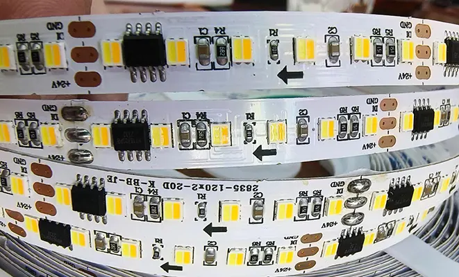
A single-sided flexible PCB consists of one conductive copper layer laminated onto a flexible insulating substrate. The most commonly used substrate material is polyimide (PI), although PET and other polymers are used in cost-driven applications.
The copper layer is typically protected by a polyimide coverlay, which provides electrical insulation and mechanical protection.
Depending on the application, local stiffeners—such as FR-4 or polyimide sheets—may be bonded to specific areas to support connectors or solder joints. Electrically, all routing is confined to a single plane, with no interlayer connections.
Typical Manufacturing Characteristics
Single-sided flex PCBs follow a relatively straightforward fabrication flow. Circuit patterns are formed by imaging and etching a single copper layer, followed by coverlay lamination and surface finishing. The absence of drilled vias or interlayer registration significantly simplifies process control.
Because there is no layer-to-layer alignment requirement, dimensional stability tolerances are looser, and yield loss from registration defects is minimal. This simplicity translates directly into shorter lead times, higher yields, and lower tooling costs, especially in high-volume production.
Common Applications
Single-sided flex PCBs are widely used in low-density and cost-sensitive applications where routing complexity is limited. Typical examples include LED lighting strips, printer cables, simple sensor interconnects, membrane switches, and battery contact circuits.
They are best suited for static installations or applications with limited bending cycles, where mechanical strain is predictable and modest.
What Is a Double-Sided Flexible PCB?
Definition and Layer Structure
A double-sided flexible PCB incorporates two conductive copper layers, separated by a flexible dielectric core. Electrical connectivity between the two layers is achieved through plated through-holes (PTHs) or microvias, enabling signal routing on both sides of the substrate.
This structure effectively doubles the available routing area without increasing the overall footprint, making double-sided flex PCBs a natural solution when single-layer designs reach their density limits.
Manufacturing Characteristics
Compared to single-sided flex PCBs, double-sided designs introduce several additional manufacturing steps. After forming inner copper patterns, the board must undergo drilling, hole wall preparation, and copper metallization to create reliable interlayer connections.
Lamination processes must be tightly controlled to ensure dielectric thickness uniformity and via integrity.
Layer-to-layer alignment becomes critical, with typical registration tolerances in the ±50 μm range. Any misalignment can result in annular ring breakout or compromised via reliability, increasing scrap risk if not properly managed.
Typical Applications
Double-sided flex PCBs are commonly used in compact electronic assemblies that require moderate to high routing density. Applications include camera modules, wearable electronics, automotive sensor circuits, medical probes, and consumer devices with constrained packaging envelopes.
They are particularly valuable where signal routing flexibility is required without moving to a full multilayer or rigid-flex solution.
Single-Sided vs Double-Sided Flex PCB Manufacturing Process Comparison
Process Flow Comparison
From a process perspective, both single-sided and double-sided flex PCBs share core steps such as copper imaging, etching, and coverlay application. However, double-sided flex fabrication introduces drilling, desmear, and plating operations that single-sided designs completely avoid.
| Manufacturing Step | Single-Sided Flex | Double-Sided Flex |
|---|---|---|
| Copper imaging & etching | Required | Required (both layers) |
| Coverlay lamination | Required | Required |
| Drilling | Not required | Required |
| Metallization / plating | Not required | Required |
| Layer alignment | Minimal | Critical |
Each added process step increases cycle time and introduces additional opportunities for variation.
Manufacturing Complexity
Tooling requirements for single-sided flex PCBs are minimal, often limited to imaging masks and coverlay cutting tools. Double-sided flex PCBs require drilling programs, plating fixtures, and tighter lamination controls. As complexity increases, so does the need for statistical process control to maintain yield stability.
In volume production, the yield gap between single- and double-sided flex boards can be significant, particularly for fine-pitch designs or thin substrates.
Reliability and Failure Risk
Reliability profiles differ markedly between the two structures. Single-sided flex PCBs have no vias, eliminating one of the most common failure modes in flexible circuits.
Double-sided flex PCBs introduce via-related risks, especially under repeated bending. Poorly designed or over-plated vias can crack due to cyclic mechanical stress, leading to intermittent or latent failures.
For applications involving dynamic flexing, via placement and copper thickness control become critical reliability factors.
Materials Used in Single-Sided and Double-Sided Flex PCB Manufacturing
Flexible Substrate Materials
Material selection strongly influences thermal performance and dimensional stability. Polyimide remains the dominant substrate for both single- and double-sided flex PCBs due to its high temperature resistance and mechanical durability.
| Material | Max Operating Temp | Dimensional Stability | Typical Use |
|---|---|---|---|
| PI (Polyimide) | 200–260°C | Excellent | High-reliability flex |
| PET | 120–150°C | Moderate | Cost-sensitive electronics |
| PEN | ~180°C | Good | Mid-range consumer devices |
| LCP | >260°C | Excellent | High-frequency, fine-line designs |
Double-sided flex designs are more sensitive to substrate stability, as any dimensional movement affects via alignment and reliability.
Copper Foil Selection
Copper foil type plays a decisive role in flex durability. Rolled annealed (RA) copper is preferred for flex applications due to its superior fatigue resistance, while electrodeposited (ED) copper is often used in cost-driven or static designs.
| Copper Type | Flex Life | Cost | Typical Application |
|---|---|---|---|
| RA copper | High | Higher | Dynamic flex zones |
| ED copper | Moderate | Lower | Static or limited flex |
Double-sided flex PCBs typically benefit more from RA copper, particularly around vias and bend regions.
Stiffener Options
Stiffeners are used to locally reinforce flexible circuits, regardless of layer count. FR-4 stiffeners are common for connector support, polyimide stiffeners maintain thermal consistency, and metal stiffeners such as stainless steel or aluminum are used for ultra-thin or high-strength requirements.
In double-sided flex PCBs, stiffener placement must be carefully coordinated with via locations to avoid stress concentration. Single-sided designs generally allow greater freedom in stiffener placement due to their simpler structure.
Electrical Performance Differences
When evaluating single-sided and double-sided flex PCBs, electrical performance is often a differentiator that goes beyond mere physical structure. The ability to route more signals, control impedance, and mitigate electromagnetic interference (EMI) directly influences how effectively a flex circuit performs in demanding applications.
Signal routing capability
Signal routing capability in a single-sided flex PCB is inherently limited by the fact that all conductors must reside on a single plane. While this constraint simplifies manufacturing, it restricts the conductor layout and often necessitates longer traces or jumpers to reach targeted components.
In contrast, double-sided flex PCBs provide two planes for signal distribution, effectively doubling the available routing area within the same footprint. This additional layer improves layout efficiency, reduces trace congestion, and permits more direct routing paths that enhance signal integrity.
Impedance control potential
Impedance control potential is closely tied to stack-up geometry and reference plane availability. Single-sided flex circuits typically rely on a ground reference provided via an external plane or return path, which can make impedance consistent only in specific, predictable layouts.
Double-sided flex PCBs can embed return paths closer to signal layers or include controlled impedance pairs with better predictability. In applications requiring high-speed data transfer or matched-impedance transmission lines, such as USB or LVDS interfaces, this inherent stack-up advantage becomes significant.
- EMI considerations
EMI considerations follow from the above. EMC performance can degrade when return current paths are distant or discontinuous, as is often the case in single-sided designs.
Double-sided flex PCBs facilitate nearer return paths and the possibility for contiguous ground references, which reduces loop area and improves immunity to radiated emissions.
Power and current-carrying limitations
Finally, power and current-carrying limitations differ between the two structures. Double-sided flex PCBs, by virtue of having distributed copper on both sides, can support wider conductor cross-sections within the same board area, enhancing current capacity marginally over single-sided designs.
However, neither type rivals the current-handling capabilities of rigid multilayer boards; thermal management and bend-area stress considerations limit the practical current capacity in all flex circuits.
Cost Comparison: Single-Sided vs Double-Sided Flex PCBs
Cost is a commercially significant decision criterion, and this section highlights the primary drivers that differentiate single-sided from double-sided flex PCB pricing.
Material cost differences begin with the obvious: double-sided flex PCBs require twice the patterned copper layers and a dielectric core between them. This increases raw material use, but more importantly, it introduces the need for plating chemistry, consumables, and the intermediate dielectric layer itself.
While the additional substrate and copper do add cost, the primary material premium arises from the process steps associated with double-sided construction.
Tooling and setup cost for double-sided flex PCBs are inherently higher. Drilling programs for plated through-holes, lamination tooling to control alignment between two patterned layers, and fixtures to support bidirectional imaging all contribute to setup overhead.
For low-volume production, these fixed costs can dominate unit pricing, whereas high-volume production can amortize tooling more effectively.
Yield and scrap rate impact also plays a role. Single-sided flex PCBs, with their simplified structure, have fewer opportunities for manufacturing variation to become a defect. In double-sided flex PCBs, misregistration, delamination, or via plating defects can occur if process controls are not robust, leading to increased scrap risk and quality rework.
When considering cost vs performance trade-offs, designers and procurement teams should view the decision as a value optimization rather than a price competition.
While single-sided designs are typically lower cost, double-sided flex PCBs often enable greater functional density, improved signal integrity, and reduced assembly complexity—attributes that can drive down overall system cost and improve product competitiveness.
Design Flexibility and Layout Constraints
Design flexibility and layout efficiency are where the practical impacts of the structural choice become most visible to PCB designers.
Trace routing limitations are immediate in single-sided flex PCB layouts. Because all conductors reside on one surface, crossing signals or dense nets often require creative loop routing, jumpers, or added connectors. This can increase both design complexity and the potential for signal integrity issues.
In double-sided flex circuits, designers can leverage the second layer to route return paths, bypass congested regions, or separate analog and digital domains more effectively.
Via placement rules are another distinguishing factor. Single-sided flex designs inherently avoid vias, which simplifies layout but restricts routing options. Double-sided flex PCBs can incorporate plated through-holes, microvias, or blind vias to interconnect signal planes, enabling more compact and efficient layouts. However, designers must carefully control via placement relative to bend regions to avoid mechanical stress concentrations and fatigue cracking.
Bend area design restrictions are governed by mechanical tolerance and stress distribution. Single-sided flexibility allows thinner, more compliant circuits; however, designers must still avoid sharp trace corners, abrupt width changes, and sudden metal density shifts that concentrate stress.
Double-sided designs, with copper on both faces, tend to be slightly stiffer. As a consequence, bends must be located in areas free from vias and ideally aligned with neutral mechanical axes defined by stack-up thickness.
Panel utilization efficiency differs as well. Single-sided flex PCBs often require more board area to accommodate equivalent functionality due to routing constraints. Double-sided flex designs, by using both surfaces, typically achieve higher packing density, improving panel utilization and reducing overall material waste.
Comparison Table: Single-Sided vs Double-Sided Flex PCB
To support featured snippet visibility and provide engineers with a quick structural comparison, the table below summarizes key differences.
| Aspect | Single-Sided Flex PCB | Double-Sided Flex PCB |
|---|---|---|
| Circuit density | Low | Medium |
| Manufacturing complexity | Low | Medium |
| Cost | Lower | Higher |
| Flexibility | Higher (thinner, more compliant) | Slightly lower (stiffer due to two copper layers) |
| Via requirement | No | Yes |
| Typical use | Simple circuits, static applications | Compact, denser designs requiring signal flexibility |
This table distills the core engineering and manufacturing distinctions in a format readily referenced by product planners, PCB designers, and procurement teams.
Single-Sided vs Double-Sided vs Multilayer Flex PCBs
As product functionality increases, the limitations of single-sided and even double-sided flex PCBs become more apparent. Understanding where one technology ends and the next begins is essential to selecting the right solution without overengineering.
Single-sided flex PCBs reach their practical limit when routing density increases to the point where signal crossovers, long trace detours, or external jumpers are required. At that stage, moving to a double-sided flex PCB is often the most efficient step, as it adds routing freedom without dramatically increasing thickness or cost.
However, double-sided flex PCBs also have clear boundaries. When the circuit requires multiple reference planes, extensive power distribution, controlled impedance across many signals, or complex interconnections within a confined footprint, two copper layers are no longer sufficient. Designers may find themselves constrained by via congestion, copper imbalance, or EMI challenges that cannot be resolved within a two-layer structure.
This is where multilayer flex PCBs become the appropriate choice. By incorporating three or more conductive layers, multilayer flex circuits provide significantly higher wiring density, improved signal integrity, and better power and ground management. They also allow designers to place sensitive signals closer to the neutral mechanical axis, improving reliability in dynamic bending applications.
In short, the transition from single-sided to double-sided flex is driven primarily by routing efficiency, while the move to multilayer flex is driven by system-level electrical performance and integration requirements.
How to Choose the Right Flex PCB Type for Your Project
Selecting the appropriate flex PCB structure should be a deliberate engineering decision rather than a default choice based on familiarity or cost alone.
Circuit complexity is often the first indicator. Single-sided flex PCBs suit simple interconnects with minimal routing. As signal count and functional integration increase, double-sided flex becomes a more natural fit. Multilayer flex PCBs become justified when two layers cannot achieve the required signal integrity, power distribution, or functional density.
Space constraints play an equally important role. In products where board area is limited but thickness must remain minimal—such as wearables or compact medical devices—double-sided or multilayer flex designs reduce footprint even if per-unit cost increases.
Mechanical flexibility requirements must be evaluated early. Applications involving repeated bending, folding, or vibration benefit from simpler structures with fewer copper layers and no vias in bend zones. While multilayer flex PCBs can be designed for dynamic motion, doing so requires advanced materials and careful stack-up optimization.
Budget considerations should be viewed holistically. While single-sided flex PCBs are the least expensive at the board level, double-sided or multilayer designs may reduce assembly complexity, connector count, or overall system size—often lowering total product cost.
Finally, delivery timeline can influence technology choice. Single-sided flex PCBs typically offer the shortest lead times due to simpler fabrication. Double-sided and multilayer flex PCBs require longer setup and qualification cycles, which should be factored into project schedules.
Common Manufacturing Challenges and Solutions
Despite their advantages, flex PCBs present manufacturing challenges that must be addressed through design and process control.
Alignment accuracy is a primary concern in double-sided and multilayer flex PCBs. Flexible substrates are more susceptible to dimensional change during thermal processing, making tight registration difficult. This challenge is mitigated through adhesive-free laminates, optimized panel support, and optical alignment systems during imaging and lamination.
Adhesive overflow can unintentionally stiffen flexible areas or contaminate pad openings. Using low-flow adhesives, precisely controlled lamination pressure, and well-defined coverlay openings helps preserve intended flexibility and solderability.
Via cracking is a known long-term reliability risk, particularly in double-sided and multilayer flex PCBs subjected to dynamic bending. Designers can reduce this risk by keeping vias out of bend zones, minimizing copper plating thickness in vias, and using rolled annealed copper for improved fatigue resistance.
Warpage during assembly often occurs when flexible circuits undergo SMT reflow without adequate support. Temporary carriers or rigid fixtures are commonly used to maintain flatness during soldering and prevent component misalignment or solder joint defects.
Addressing these challenges requires close collaboration between design, manufacturing, and assembly teams—especially as flex circuit complexity increases.
Conclusion: Which Flex PCB Manufacturing Option Is Right for You?
Single-sided, double-sided, and multilayer flex PCBs each serve a distinct role in modern electronics. Single-sided flex PCBs offer simplicity, high flexibility, and low cost for straightforward interconnects. Double-sided flex PCBs strike a balance between manufacturability and routing capability, enabling compact designs with moderate complexity. Multilayer flex PCBs deliver the highest performance and integration potential, albeit with increased process complexity and cost.
For engineers and buyers, the right choice depends on a clear understanding of functional requirements, mechanical constraints, cost targets, and production timelines. Selecting the simplest structure that reliably meets performance needs is often the most effective strategy.
For readers interested in deeper technical detail, related topics worth exploring include multilayer flex PCB manufacturing processes and rigid-flex PCB design principles, both of which extend the concepts discussed in this article and support more advanced product architectures.
References
IPC-2223 – Sectional Design Standard for Flexible Printed Boards
IPC-6013 – Qualification and Performance Specification for Flexible Printed Boards
IPC-4101 – Specification for Base Materials for Printed Boards
DuPont™ Kapton® Polyimide Film Technical Guide
ASM Handbook, Volume 16 – Electronics Materials and Processes
Altium Designer – Flex and Rigid-Flex PCB Design Guidelines
Rogers Corporation – Flexible Circuit Materials Application Notes

