Mastering Flex PCB Bend Radius Calculation for Long-Life Circuits


Mechanical design is a cornerstone of flex printed circuit board (PCB) reliability, directly influencing the device’s operational lifespan and performance.
Among the key mechanical factors, the bend radius—the minimum radius a flex circuit can be bent without damage—is critical.
A well-specified bend radius minimizes mechanical stress, reducing the risk of copper trace fatigue and dielectric cracking.
Poor management of bend radius can lead to circuit failures, costly recalls, and operational downtime, underscoring the importance of informed design practices.
This document offers actionable guidance, grounded in industry data and standards, to help engineers and designers optimize flex PCB reliability.
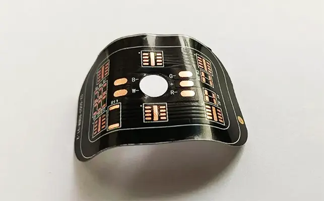
What Is Bend Radius in Flex PCBs?
Bend radius refers to the minimum allowable curvature for a flex PCB, ensuring that the circuit can be flexed without mechanical or electrical failure.
There are two primary types: static bend radius, where the circuit is bent into place and left stationary, and dynamic bend radius, where repeated flexing occurs during normal operation.
When a flex circuit bends, the outer layers experience tensile (stretching) stress, while the inner layers are subject to compressive stress.
The balance of these forces determines the mechanical integrity of the circuit over time.
The IPC-2223 standard provides widely accepted guidelines for minimum bend radii: for single-layer circuits, the recommended static bend radius is typically 6 times the circuit thickness (6×T), and for dynamic applications, 12 times the thickness (12×T).
These recommendations are critical, as exceeding them can accelerate fatigue, leading to premature failure.
As such, proper bend radius specification is often the deciding factor for long-term circuit performance.
Key Factors Affecting Bend Radius
Material Properties
The choice of base material significantly influences permissible bend radius.
Polyimide films, commonly used in flex PCBs, offer superior flexibility, high-temperature resistance (up to 260°C), and excellent chemical stability, outperforming polyethylene terephthalate (PET), which is less flexible and suited to lower temperature environments. Copper type also plays a pivotal role.
Rolled annealed (RA) copper offers greater ductility and fatigue resistance compared to electrodeposited (ED) and high ductility electrodeposited (HDED) copper, making RA preferable for repeated flexing and dynamic applications.
The fatigue life (N) of copper can often be estimated using the Coffin-Manson relationship:
N = C × (Δε)^-k
Where Δε is the strain range, C and k are material constants. RA copper typically endures higher strain cycles before failure, extending circuit longevity.
Layer Count and Stack-Up
Flex PCBs are available in single, double, and multilayer constructions, as well as rigid-flex hybrids.
As the layer count increases, the minimum bend radius must also increase due to the compounded thickness and stress distribution.
The neutral axis—an imaginary line within the stack-up where strain is zero during bending—should ideally align with the most sensitive traces. Careful stack-up design can minimize mechanical stress and enhance reliability.
Trace Design and Routing
Sharp corners and abrupt routing transitions concentrate stress, increasing the risk of trace fracture. Employing curved traces and radiused bends distributes stress more evenly.
Trace width and spacing must be optimized for both electrical performance and mechanical durability. Mechanical reinforcement, such as stiffeners or additional coverlays, can further protect vulnerable regions.
Environmental Conditions
Operational environments impose additional demands on flex circuits.
Temperature cycling can induce expansion and contraction, while vibration and humidity accelerate fatigue and corrosion.
Protective coatings and encapsulation materials can shield sensitive areas, extending circuit life under harsh conditions.
| Flex Circuit Type | Static Bend Radius | Dynamic Bend Radius |
|---|---|---|
| Single-layer | 6 × thickness (T) | 12 × thickness (T) |
| Double-layer | 12 × thickness (T) | 24 × thickness (T) |
| Multilayer (>2 layers) | 24 × thickness (T) | 48 × thickness (T) |
In summary, appropriate bend radius selection—guided by material properties, construction, and environmental factors—is crucial to achieving reliable, long-lasting flex PCB designs.
How to Calculate Bend Radius for Long-Life Circuits
The minimum bend radius for a flex PCB can be estimated using a straightforward formula:
Minimum Bend Radius ® = k × T
Where:
- R is the minimum bend radius
- T is the total thickness of the flex circuit
- k is a constant based on application and layer count (per IPC-2223)
For example, using IPC-2223 guidelines:
- Single-layer static: R = 6T
- Single-layer dynamic: R = 12T
- Double-layer static: R = 12T
- Double-layer dynamic: R = 24T
- Multilayer static: R = 24T
- Multilayer dynamic: R = 48T
Example Calculation:
Suppose a single-layer flex PCB is 0.15 mm thick. For a static application:
R = 6 × 0.15 mm = 0.9 mm
For a double-layer flex of the same thickness in a dynamic application:
R = 24 × 0.15 mm = 3.6 mm
Designers should also adjust the bend radius upward for dynamic bends (repeated flexing) to prevent fatigue failure.
Software tools (such as SolidWorks, Altium Designer, or dedicated FEA packages) can simulate stress distribution and predict fatigue life, facilitating optimal bend radius selection during the design phase.
Case Study – Wearable Electronics:
In a wearable fitness tracker, engineers optimized the flex PCB bend radius by simulating repeated flex cycles at various curvatures.
By increasing the bend radius from 1.0 mm to 1.8 mm in a dynamic region, the product’s flex circuit lifespan was extended by over 200%, illustrating the value of data-driven optimization.
Common Bend Radius Mistakes to Avoid
Several recurring mistakes can compromise flex PCB reliability:
- Neglecting the distinction between static and dynamic bend requirements can lead to premature fatigue.
- Choosing unsuitable base materials or copper types for the intended operating environment can result in cracking or delamination.
- Implementing sharp corners or abrupt trace direction changes, which concentrate mechanical stress and increase the risk of fracture.
- Failing to run thorough design rule checks (DRCs) around bend zones can leave undetected issues in the layout.
- Underestimating the effects of real-world stresses such as temperature fluctuations, vibration, and humidity.
Mechanical Design Best Practices for Flex PCBs
To maximize reliability, incorporate these best practices:
- Position sensitive signal layers as close as possible to the neutral axis to minimize strain during bending.
- Stagger trace routing between layers and maintain adequate trace separation to reduce stress coupling.
- Use radiused corners for all bends and consider adding dummy traces or teardrops at transition points for added reinforcement.
- In high-speed/frequency circuits, account for controlled impedance and EMI by maintaining consistent geometry even in bend areas.
- Collaborate early with PCB manufacturers to ensure your design meets both DFM and long-term reliability standards.
Testing and Validation for Bend Reliability
Comprehensive validation is essential for flex PCBs expected to endure repeated bending:
- Perform bend cycle (flex life) testing to quantify the number of cycles to failure under specified conditions.
- Conduct thermal cycling and environmental stress tests to evaluate performance under temperature, humidity, and vibration extremes.
- Use visual inspection, X-ray, or other non-destructive methods to identify cracks or delamination in bend zones.
- Benchmark results against IPC-2223 standards to ensure compliance and competitive reliability.
Advanced Strategies for Long-Life Flex PCBs
Pushing flex PCB reliability further, advanced strategies focus on both material engineering and system-level design.
The integration of rigid-flex architectures is one of the most effective ways to minimize high-stress regions, as rigid sections can anchor connectors or components and keep the flex portions free from excessive mechanical loads.
This approach is especially useful in applications that demand repetitive bending or where board real estate is limited.
Material selection continues to play a vital role in durability. High-ductility copper, such as rolled annealed (RA) copper, is favored for dynamic flex regions because it can endure more strain cycles before failure, as described by the Coffin-Manson relationship for fatigue life:
N = C × (Δε)^-k
where N is the number of cycles to failure, Δε is the strain range, and C and k are material constants for the chosen copper type.
Adhesiveless constructions further enhance mechanical reliability by eliminating the weakest interface in the stack-up and allowing for thinner, more flexible designs.
These improvements are especially evident in high-layer-count or high-speed circuits, where maintaining signal integrity is paramount.
Optimizing the layer stack-up is critical in advanced flex and rigid-flex designs. For high-speed or high-power applications, engineers must balance electrical requirements, such as controlled impedance, with mechanical needs like neutral axis alignment.
Simulation-driven design is now standard practice, using finite element analysis (FEA) and signal integrity software to identify potential failure points, optimize layer placement, and validate bend radii before fabrication.
These digital tools allow for rapid iteration and data-driven decision making, dramatically improving long-term reliability and performance.

Flex PCB Bending Test
Industry Applications and Case Examples
The demand for robust flex PCB performance spans multiple industries, each presenting unique reliability challenges. In wearables and medical devices, circuits must survive repeated bending, twisting, and exposure to sweat or cleaning fluids.
Advanced materials, careful routing, and simulation-driven bend radius optimization have enabled devices like fitness trackers and implantable sensors to achieve lifespans measured in millions of cycles.
Automotive and advanced driver-assistance systems (ADAS) put flex circuits through extreme vibration and thermal cycling.
Here, rigid-flex integration, thick polyimide substrates, and protective encapsulation are combined to maintain signal integrity and mechanical function under continuous stress.
In the aerospace and satellite sector, flex PCBs face both temperature extremes and high-cycle fatigue. Thorough pre-qualification—using accelerated bend and thermal cycling tests—ensures mission-critical reliability, often exceeding the minimum standards set by IPC-2223.
Consumer electronics, such as foldable phones, laptops, and compact cameras, represent another area where flex PCB innovation is paramount.
Engineers employ ultra-thin stack-ups, high-ductility copper, and precision simulation to meet aggressive form factor and lifecycle requirements.
In all these applications, the core principles of bend radius calculation, robust material selection, and validation testing remain central to success.
Conclusion
Across all sectors, the bend radius stands out as the single most critical design parameter guiding flex circuit longevity.
When combined with informed choices in materials, layer stack-up, routing, and standardized validation, designers can dramatically reduce field failures and warranty risks.
Early collaboration with manufacturing partners ensures that designs are both manufacturable and robust, while strict adherence to IPC standards further safeguards long-term reliability.
Ultimately, a well-calculated bend radius is the foundation for flex circuits that excel under mechanical stress and deliver reliable performance throughout their operational life.

