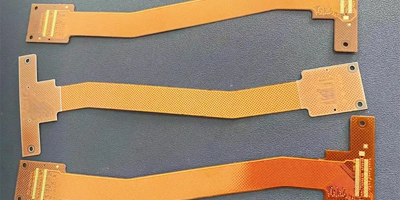
Flex PCB Design Guidelines and Best Practices for Maximum Reliability


Flexible PCBs are rarely chosen for cost reasons. They are chosen because rigid boards cannot survive the mechanical constraints of the product. Ironically, this is also why flex PCB failures are often more expensive and harder to repair than rigid PCB failures.
When a rigid PCB fails, the root cause is usually electrical: overstress, overheating, or poor solder joints. In contrast, flex PCB failures are mechanical in origin, even when they manifest electrically.
Typical failure modes include copper cracking, coverlay delamination, pad lift, and plated-through hole barrel fracture. These failures often occur after assembly or during field use, making rework impractical or impossible.
The challenge is that many engineers still apply rigid PCB thinking to flexible circuits—optimizing impedance, current capacity, or routing density—while underestimating mechanical strain. This mismatch is the primary reason flex PCBs fail prematurely.
From a reliability standpoint, flex PCB design is less about routing convenience and more about strain management, material behavior, and fatigue life.
Flex PCB Design: Static vs Dynamic – Define Before You Design
Before selecting materials or calculating bend radius, one question must be answered clearly:
Will the flex circuit bend once, or bend repeatedly?
This distinction is frequently mentioned in competitor articles, but rarely structured properly—yet it determines nearly every downstream design decision.
Static Flex (Bend-to-Install)
Static flex circuits are designed to bend once or only a few times, typically during assembly. After installation, the circuit remains mechanically stable for its entire service life.
Typical applications include camera modules, connector interposers, and tight enclosures where a rigid PCB cannot fit. In these designs, fatigue life is not the dominant concern—strain during initial forming is.
Static flex allows more relaxed rules for copper thickness, bend radius, and via placement, but failures still occur when designers underestimate the strain introduced during final assembly.
Dynamic Flex (Continuous Bending)
Dynamic flex circuits experience repeated bending cycles, ranging from thousands to millions over product life. Examples include printer heads, laptop hinges, wearable devices, and robotic joints.
In these applications, copper fatigue becomes the limiting factor. Even small design violations—such as the wrong copper type or a slightly undersized bend radius—can reduce lifetime by orders of magnitude.
Dynamic flex design is unforgiving. Rules that are “acceptable” in static flex often become prohibited.
Static vs Dynamic Flex – Reliability Comparison
| Parameter | Static Flex | Dynamic Flex |
|---|---|---|
| Bend cycles | < 100 | 10,000 – millions |
| Copper type | RA recommended | RA mandatory |
| Typical bend ratio | ≥ 10:1 | 20:1 – 100:1 |
| Vias in bend area | Strongly discouraged | Prohibited |
| Failure mechanism | Over-strain | Copper fatigue |
Bend Radius Rules – The #1 Cause of Flex PCB Failure
Most flex PCB failures can be traced back to one issue: insufficient bend radius. Many articles quote ratios without explaining why they matter, which leads to blind rule-following instead of robust engineering.
Bend Radius and the Neutral Axis (Simple Explanation)
When a flex PCB bends, the outer layers stretch while the inner layers compress. Between them lies the neutral axis—the zone where mechanical strain is theoretically zero.
Copper cracks when tensile strain exceeds its fatigue limit. Therefore, the closer copper is to the neutral axis, the longer it survives.
Poor stackup symmetry or thick adhesive layers can shift the neutral axis toward one copper layer, dramatically increasing strain even if the bend radius appears compliant on paper.
IPC-2223 Bend Ratio Guidelines
IPC-2223 provides conservative, field-proven guidelines that correlate bend radius to total flex thickness.
| Flex Type | Minimum Bend Ratio (Radius : Thickness) |
|---|---|
| Single-layer static | 10:1 |
| Double-layer static | 15:1 |
| Dynamic flex | 20:1 – 100:1 |
For dynamic applications, the wide range reflects differences in copper thickness, cycle count, and acceptable failure probability.
Practical Engineering Rules (Beyond IPC)
In practice, many failures occur even when IPC ratios are met, due to poor implementation. Reliable designs follow these additional principles:
Sharp 90-degree folds create localized strain concentration and should be avoided entirely. Bends should be formed, not creased.
Traces should always run perpendicular to the bend axis to prevent tensile loading along the copper grain.
Mechanical forming tools or bend fixtures should be used for repeatability during assembly.
Material Selection – The Foundation of Reliability
Materials do not fail randomly. Each flex PCB material choice maps directly to specific failure mechanisms. Understanding this relationship is what separates reliable designs from marginal ones.
Polyimide vs PET – Application-Driven Choice
Polyimide (PI) is the industry standard for high-reliability flex circuits due to its thermal stability, chemical resistance, and fatigue performance. It is essential for medical, automotive, and aerospace applications.
PET, while cheaper, has lower temperature tolerance and poorer long-term mechanical stability. It is suitable only for low-cost consumer products with limited bending cycles and controlled environments.
Rolled-Annealed (RA) vs Electro-Deposited (ED) Copper
This is one of the most critical—and misunderstood—decisions in flex PCB design.
RA copper has an elongated grain structure that aligns with bending, allowing it to deform plastically over many cycles without cracking.
ED copper has a columnar grain structure that creates stress concentration points, leading to early fatigue failure under cyclic bending.
For dynamic flex, ED copper is not a cost optimization—it is a reliability risk.
Adhesiveless vs Adhesive-Based Stackups
Adhesive layers introduce moisture absorption, thermal mismatch, and long-term creep. These effects reduce plated via reliability and accelerate delamination under thermal cycling.
Adhesiveless constructions place copper directly on polyimide, improving dimensional stability, via integrity, and high-temperature performance—especially important for lead-free assembly.
Coverlay Design Rules That Prevent Tearing
Coverlay is not a solder mask; it is a structural element. Poor coverlay window design often initiates cracks that propagate into copper.
Openings should be oversized to prevent stress concentration. Overlap onto pads must be sufficient to prevent peel-back. Sharp internal corners should be avoided entirely, as they act as crack initiators during bending.

Material Selection
Stackup Design Best Practices (Single, Double, Multilayer, Rigid-Flex)
Stackup design determines where strain accumulates. Many flex PCBs fail not because of routing errors, but because the stackup amplifies mechanical stress.
Single-Layer Flex Stackup
Single-layer flex offers the highest reliability for dynamic applications. With copper close to the neutral axis and minimal thickness, strain is inherently limited.
This structure is preferred whenever routing density allows, particularly in high-cycle environments.
Double-Layer Flex – Balanced Construction
In a double-layer flex, copper symmetry is essential. Unequal copper thickness or asymmetric adhesives shift the neutral axis, increasing strain on one layer.
Balanced stackups dramatically improve fatigue life without increasing bend radius.
Multilayer Flex – Avoiding the I-Beam Effect
Multilayer flex circuits are prone to the “I-beam” effect, where stiff outer layers concentrate stress in the center. The bookbinding technique—staggering layer lengths—allows each layer to flex independently, reducing peak strain.
Rigid-Flex Transition Zones
The rigid-to-flex interface is a common failure site. Best practice requires a via keep-out of at least 50 mil from the transition, no components near the bend line, and only filleted (never sharp) board outlines.
Layout & Routing Rules for Maximum Mechanical Reliability
Flex PCB routing is not primarily an electrical exercise. It is a strain management problem expressed through copper geometry. The goal of layout is not simply connectivity, but ensuring that copper deforms elastically—and predictably—throughout the product’s life.
Trace Routing in Bend Areas
The direction of copper relative to the bend axis determines whether it experiences tensile fatigue or benign flexure. Traces routed parallel to the bend line experience maximum tensile strain and are the most common root cause of copper cracking.
For reliable designs, traces should always cross the bend perpendicular to the bend axis, allowing strain to distribute across the trace width rather than along its length. This significantly improves fatigue life, especially in dynamic flex applications.
Right-angle corners create localized strain concentration points that act as crack initiation sites. In flex, these effects are amplified compared to rigid PCBs. Replacing corners with arcs or spline-based curves allows strain to distribute smoothly during bending.
Trace width transitions must also be gradual. Sudden neck-downs or expansions shift strain abruptly, increasing the likelihood of micro-cracks at transition points. A taper length of at least 3× the trace width is commonly used in high-reliability designs.
Via Design in Flex Circuits
Vias are rigid structures embedded in a flexible system, and their presence fundamentally disrupts strain continuity. This is why vias in bend zones are a leading cause of early failure.
In reliable flex designs, vias are completely excluded from bend areas, not merely “discouraged.” Even when IPC allowances appear to permit them, field data consistently shows reduced fatigue life when vias experience repeated flexing.
Outside bend zones, vias should use larger-than-rigid annular rings to account for material movement and plating stress. Teardrops are not cosmetic in flex PCBs; they are a structural requirement that reduces stress concentration at the trace-to-pad interface, especially during thermal cycling and bending.
Pad Design and Mechanical Reinforcement
Isolated pads—pads connected only by narrow traces—are highly susceptible to pad lift in flex circuits. During bending or reflow, these pads experience localized stress without adequate copper anchoring.
Best practice is to mechanically anchor pads to the surrounding copper whenever possible. This does not mean flooding copper indiscriminately, but rather providing controlled reinforcement paths that allow stress to dissipate.
For double-sided flex, placing pads directly opposite each other creates a local stiffness spike that shifts the neutral axis. Staggering pads between layers helps preserve uniform flexibility and reduces interlayer stress.
Plane Design: Ground and Power in Flex
Large copper planes improve electrical performance but reduce flexibility. This creates a fundamental tradeoff between mechanical reliability and EMI control.
Solid copper planes significantly stiffen the flex region and should be avoided in dynamic bend areas. Cross-hatched planes reduce bending stiffness while still providing acceptable return paths for many signal types. However, hatch geometry must be designed carefully to avoid resonant EMI behavior.
For high-speed or sensitive analog circuits, localized solid planes may be acceptable if they are kept outside bend zones and transition smoothly into flexible regions.
Stiffener Design – Where, Why, and How
Stiffeners are often treated as an afterthought, yet they play a critical role in stress redistribution and assembly reliability. Poor stiffener placement can cause more harm than good.
What Stiffeners Actually Do (Mechanical Perspective)
Mechanically, stiffeners do not “strengthen” flex PCBs—they relocate stress. By increasing local stiffness, they force bending to occur elsewhere. When placed correctly, this protects sensitive areas such as connector interfaces and solder joints. When placed incorrectly, they concentrate stress at their edges.
Stiffeners are also essential for connector support, ensuring coplanarity during insertion and preventing pad damage under insertion force.
Common Stiffener Materials and Their Behavior
FR4 stiffeners are widely used due to cost and availability. They provide high rigidity but introduce a sharp stiffness transition if not properly filleted.
Polyimide stiffeners offer better CTE matching and smoother mechanical transitions, making them suitable for higher-reliability or thinner constructions.
Stainless steel stiffeners are used where maximum rigidity is required in minimal thickness, such as ZIF connector reinforcement, but they demand careful edge treatment to avoid stress risers.
Placement Rules That Prevent Failure
Stiffeners must never intersect a bend line. Doing so creates a hinge point at the stiffener edge, dramatically increasing copper strain.
They should be used only where rigidity is functionally required—typically under connectors or component zones—and their edges should always be filleted or tapered to soften stiffness transitions.
EMI, Impedance, and High-Speed Design in Flex PCBs
One of the most overlooked aspects of flex PCB design is that mechanical variability directly affects electrical performance. High-speed design rules cannot simply be copied from rigid boards.
Controlled Impedance Challenges in Flex
In flex circuits, dielectric thickness varies more than in rigid PCBs due to adhesive flow, coverlay tolerance, and material stretch during lamination. This variability directly impacts impedance control.
Reliable controlled-impedance flex designs rely on adhesiveless stackups, tight material control, and impedance modeling that accounts for bending-induced geometry changes—especially in dynamic applications.
Shielding Options and Mechanical Tradeoffs
Solid copper shielding provides excellent EMI suppression but severely reduces flexibility. Cross-hatched shielding offers a compromise, maintaining acceptable shielding effectiveness while allowing bending.
Shield films and embedded shielding layers can also be used, particularly in rigid-flex designs where shielding is confined to rigid sections and transitions carefully into flex regions.
Differential Pair Routing in Flex
Differential pairs must remain geometrically symmetrical throughout the flex region to maintain impedance balance. Any asymmetry introduced by bending, layer transitions, or inconsistent coverlay openings can degrade signal integrity.
In bend zones, differential pairs should avoid transitions, vias, and layer changes entirely. Bends should be gradual and uniform across both traces to prevent skew and mode conversion.
Manufacturing & Assembly Considerations (DFM/DFA)
Even a perfectly designed flex PCB can fail if manufacturing and assembly realities are ignored. Many reliability issues originate after design freeze, during handling and assembly.
Panelization of Flex PCBs
Flex circuits are rarely processed as standalone parts. Temporary carriers, stiffener frames, or rigid backers are used to enable SMT assembly.
Poor panelization design leads to handling damage, registration issues, or uneven reflow profiles. Break-away tabs must be designed to release cleanly without inducing tearing or delamination.
Handling, Storage, and Baking
Flex PCBs absorb moisture more readily than rigid boards, particularly adhesive-based constructions. Moisture trapped during reflow can cause delamination, blistering, or pad lift.
Pre-baking is often required before assembly, especially for fine-pitch or high-reliability applications. Baking profiles should follow material supplier guidelines rather than generic rigid PCB rules.
Common Manufacturing Defects and Their Root Causes
Pad lift typically results from poor pad anchoring combined with thermal stress during reflow.
Barrel cracking is most often linked to vias placed too close to bend zones or excessive Z-axis expansion.
Coverlay misalignment can expose copper edges, creating crack initiation points during bending.
Understanding these defects allows designers to eliminate them at the layout stage, rather than relying on inspection to catch them later.
Testing & Reliability Validation
Design intent alone does not guarantee reliability. Flex PCBs must be validated under mechanical and thermal conditions that reflect real use, not just electrical functionality. Unfortunately, many projects skip or underperform this step, discovering failures only after field deployment.
Bend Cycle Testing
Bend cycle testing is the most direct way to validate flex PCB fatigue life. The circuit is bent repeatedly to a defined radius while continuity and resistance are monitored in real time.
For dynamic flex applications, testing typically ranges from 10,000 cycles for consumer products to over 1 million cycles for industrial or medical devices. Failures usually initiate as micro-cracks in copper traces, which manifest as intermittent opens long before complete fracture.
Meaningful results require that the test bend radius, speed, and direction accurately reflect the actual product mechanics. Overly generous test conditions provide false confidence.
Thermal Shock and Thermal Cycling
Thermal shock testing exposes flex PCBs to rapid temperature transitions, stressing the interfaces between copper, polyimide, adhesives, and plated vias.
Typical profiles cycle between extreme temperatures (for example, −40 °C to +125 °C) with minimal dwell time. These tests reveal weaknesses such as barrel cracking, coverlay delamination, and pad lift—especially in adhesive-based constructions.
Thermal cycling with longer dwell times is often used to simulate long-term field aging, particularly for automotive and industrial environments.
Peel Strength Testing
Peel strength measures the adhesion between copper and the base material. While often overlooked, it is a critical indicator of long-term reliability, especially in dynamic applications.
Low peel strength increases the risk of trace lift during bending, handling, or rework. Adhesiveless polyimide constructions generally exhibit more stable peel performance over temperature and humidity exposure compared to adhesive-based systems.
IPC-6013 Requirements
IPC-6013 defines performance and qualification requirements specifically for flexible printed circuits. It classifies flex PCBs into different performance classes, with Class 2 covering general electronics and Class 3 targeting high-reliability applications.
Compliance with IPC-6013 does not guarantee zero failures, but it establishes minimum acceptable mechanical, electrical, and material standards. Designs intended for dynamic bending or harsh environments should always be validated against Class 3 criteria.
Common Flex PCB Design Mistakes (and How to Avoid Them)
Most flex PCB failures are not alluring or unavoidable. They result from repeatable design mistakes that appear across industries and experience levels.
Vias placed in bend zones remain the most common and destructive error. Even when electrical performance appears unaffected initially, fatigue failure is almost inevitable under repeated bending.
Sharp trace corners act as crack initiators. In flex, the penalty for ignoring this is far higher than in rigid boards.
Overlapping pads on opposite layers create local stiffness spikes that distort the neutral axis, increasing copper strain during bending.
Vias placed near stiffener edges experience concentrated stress due to abrupt stiffness transitions. These vias often fail during thermal cycling rather than mechanical bending.
Solid copper pours in dynamic areas dramatically reduce flexibility and accelerate fatigue. While they improve EMI performance, they must be restricted to non-bending regions.
Finally, the absence of strain relief—both electrically and mechanically—causes stress to accumulate at connectors and solder joints, leading to early field failures.
Avoiding these issues requires intent, not heroics. Most can be eliminated during layout review if mechanical behavior is considered as seriously as electrical rules.
When NOT to Use Flex PCB (Engineer Honesty Builds Trust)
Flex PCBs are powerful, but they are not a universal solution. In some cases, using flex adds cost and risk without meaningful benefit.
High-current applications often exceed the practical copper thickness and thermal dissipation limits of flex materials. Rigid boards or busbar solutions are usually more reliable.
Environments involving continuous abrasion, scraping, or uncontrolled mechanical contact can damage coverlay and expose copper, making flex unsuitable without extensive protection.
Ultra-low-cost, high-volume consumer products often cannot absorb the material and process costs of flex, especially when bending is minimal or unnecessary.
Most importantly, if there is no genuine space constraint or mechanical requirement, a rigid PCB will almost always be simpler, cheaper, and easier to manufacture.
Knowing when not to use flex is a hallmark of experienced engineering—not a limitation.
Flex PCB vs Rigid-Flex vs Rigid – Selection Guide
Choosing the correct interconnect technology is a system-level decision that balances cost, reliability, and mechanical needs.
| Parameter | Flex PCB | Rigid-Flex | Rigid PCB |
|---|---|---|---|
| Cost | Medium | High | Low |
| Reliability | High (with correct design) | Very high | High |
| Assembly complexity | Complex | Complex | Easy |
| Space saving | Excellent | Excellent | Limited |
| Mechanical integration | Excellent | Excellent | Poor |
Rigid-flex designs often provide the best overall reliability by confining bending to controlled flex regions while maintaining rigid support for components and connectors.
Conclusion – Reliability Is a System, Not a Rule List
Reliable flex PCB design cannot be reduced to a checklist. It is the result of aligned decisions across materials, stackup, routing, manufacturing, assembly, and handling.
Ignoring any one of these elements shifts stress elsewhere, often to a location that fails silently and late. Successful designs treat mechanical behavior as a first-class design constraint from concept through validation.
For engineers and teams working with flex circuits, the most effective next steps are practical ones:
Download a flex PCB DFM and reliability checklist
Request an independent design-for-reliability review
Engage with manufacturing engineers early, not after layout is frozen
Flex PCBs can deliver exceptional reliability—but only when they are engineered as mechanical systems, not just electrical interconnects.

