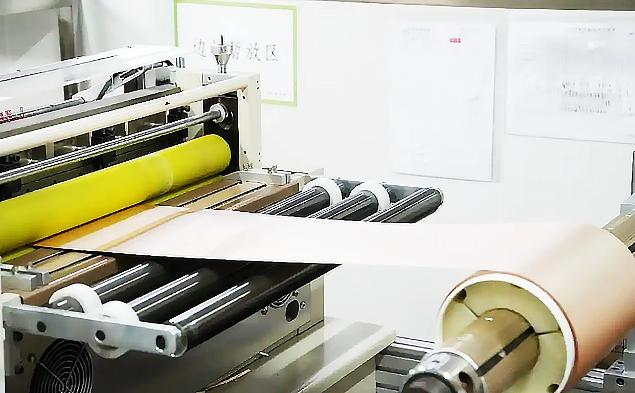
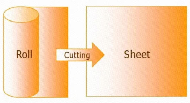
Flexible PCB Material Preparation: Cutting process


Introduction
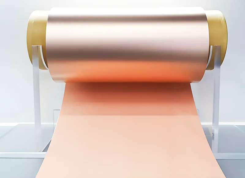
Flexible materials come in rolls. The material is cut to the needed size based on the MI size
Material preparation is the first and critical step in any flex PCB manufacturing process.
Proper material preparations reduce defects in later steps.
This guide focuses on cutting and cleaning.
It explains materials, methods, controls, and best practices.
Engineers and procurement teams will find practical, actionable advice.
Why Material Preparation Matters
Material prep affects yield and reliability.
Incorrect prep causes alignment issues in the etch process.
Contaminants cause poor adhesion of adhesive layers.
Poor cutting damages the substrate material edges.
All these issues affect electrical connections later.
For high quality flex PCBs, prep must be strict and repeatable.
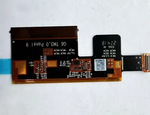
Common Materials Used
The most common materials in flexible circuits are listed below.
| Material | Function | Notes |
|---|---|---|
| Polyimide films | Flexible substrate and base material | Standard choice for thermal stability and flexibility. |
| Copper foil | Conductive traces for circuit pattern | Thickness varies by PCB designs and current needs. |
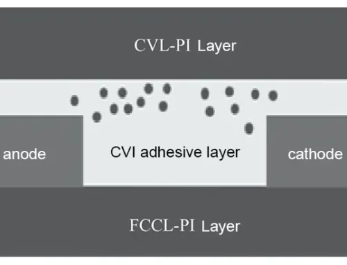
| Adhesive layers | Bond copper to substrate | Critical for multilayer and rigid flex PCB stacks. |
| Coverlay / Solder mask | Protects traces and pads | Coverlay is common for flex; solder mask is used on some rigid-flex areas. |
These flexible materials form the backbone of any flex board.
People prefer polyimide-based materials when they need flexibility and heat resistance.
Step-by-Step: Material Preparations (Detailed)
Below is a practical workflow used by production teams.
Incoming material inspection
Verify copper thickness and surface finish.
Confirm polyimide sheets match specs.
Check for coating defects and contamination.
Conditioning and drying
Bake polyimide films if needed to remove moisture.
Moisture increases the risk of delamination and solder defects.
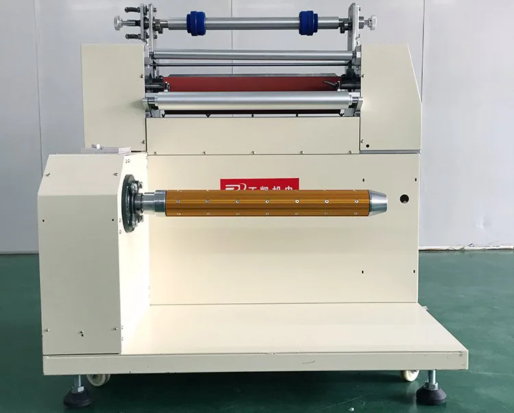
Flex PCB cutting to panel size
Cut panels to production dimensions before lamination.

Use precision flex PCB cutting to maintain tolerances.
Mark fiducials and registration points for later steps.
Edge trimming and beveling
Remove oxidized or uneven edges.
Beveled edges improve alignment in lamination and drilling.
Surface cleaning (PCB cleaning process)
Remove oils, particulates, and residues.
Methods include solvent, alkaline wash, ultrasonic, and DI rinse.
For high-reliability boards, use plasma cleaning to increase surface energy.
Final inspection and storage
Inspect for micro-scratches and particulates.
Store in dry, controlled conditions until use.
Each step in the manufacturing process must have clear acceptance criteria.
Record measurements to maintain traceability.
Flex PCB Cutting Methods and Considerations
Selecting the right cutting method depends on pcb designs and volume.
Shearing / Guillotine
Fast and economical for simple panels.
Risk of delamination on delicate layers.
CNC routing
Good for medium complexity.
Produces clean edges with repeatable tolerances.
Laser cutting
Best for tight tolerances and complex shapes.
Minimizes mechanical stress on polyimide films.
Die punching
Efficient for high-volume single shapes.
Limited to simpler outline geometries.
When cutting, maintain flatness and tension control.
Poor flex PCB cutting can distort the circuit pattern and affect registration.
PCB Cleaning Process: Methods & Why They Matter
A rigorous PCB cleaning process prevents defects in plating and adhesion.
Solvent degreasing removes oils from handling.
Alkaline cleaning removes flux residues and organic contaminants.
Ultrasonic cleaning aids in removing particles from crevices.
Plasma cleaning raises surface energy for better adhesion.
DI water rinse prevents ionic residues.
Clean surfaces ensure adhesive layers bond properly.
They also reduce voids under the solder mask or coverlay.
Contamination left behind can later cause intermittent electrical connections.
Inspection and Quality Control for Material Prep
QC must be measurable and fast.
Dimensional check for panel size and hole placement.
Surface inspection under magnification for particles.
Contact angle measurement for surface energy after cleaning.
Moisture content test for polyimide base material.
Adhesion tape test for laminate strength.
Document each lot and tie results to downstream performance.
This data helps optimize the flex PCB manufacturing process.
Impact on Downstream Processes
Good material prep simplifies later steps.
Accurate cutting improves alignment during circuit pattern imaging.
Clean surfaces reduce defects in the etch process and plating.
Stable substrate reduces warpage in lamination and soldering.
Proper edges reduce burrs that can short traces.
For rigid-flex PCBs, material preparation is even more critical.
It ensures rigid and flexible sections join without stress.
Best Practices Checklist
Use the following checklist to standardize prep.
Inspect incoming sheets and foils.
Bake polyimide films when needed.
Choose the cutting method per design tolerance.
Clean using a validated multi-stage process.
Measure surface energy after cleaning.
Store materials in dry cabinets.
Track lot numbers and inspection data.
Follow this checklist to reach high quality outputs consistently.
Common Problems and How to Fix Them
| Problem | Likely Cause | Fix |
|---|---|---|
| Delamination | Moisture in substrate | Bake and control humidity |
| Poor plating | Residue on copper | Improve cleaning and rinsing |
| Edge fray | Improper cutting | Switch to laser or CNC |
| Adhesive bubbles | Contamination or trapped air | Clean the surface and control the lamination pressure |
Address each problem early in the flow.
Prevention is less costly than rework.
Conclusion & Next Step
Material preparation sets the tone for the entire board lifecycle.
Accurate flex PCB cutting and a validated PCB cleaning process reduce defects.
They improve yield in drilling, plating, and etching.
Next in this series: PCB Drilling Process
FAQ
1. Why is material preparation important in flex PCB manufacturing?
Material preparation is the foundation of flex PCB quality. Proper cutting, cleaning, and handling reduce defects such as delamination, poor adhesion, and alignment errors—directly improving yield, reliability, and electrical performance.
2. What are the main materials used in flexible circuit boards?
The key materials include:
Polyimide film – the flexible base layer for stability and heat resistance.
Copper foil – conducts electrical signals.
Adhesive layers – bond copper to the substrate.
Coverlay or solder mask – protect traces and pads.
These materials form the essential structure of all flexible circuits.
3. What steps are involved in flex PCB material preparation?
The main process includes:
Incoming material inspection
Conditioning and drying
Cutting to panel size
Edge trimming and beveling
Surface cleaning
Final inspection and storage
Each step has acceptance criteria to ensure traceability and consistent quality.
4. Why is cutting accuracy critical for flex PCB materials?
Accurate cutting maintains panel flatness, prevents stress on polyimide films, and ensures proper alignment during imaging, lamination, and drilling. Poor cutting can cause edge fray, delamination, and misregistration in later stages.
5. What cutting methods are commonly used for flex PCB materials?
Shearing/Guillotine – fast for simple panels but risks delamination.
CNC Routing – clean and precise for moderate complexity.
Laser Cutting – ideal for tight tolerances and complex outlines.
Die Punching – efficient for high-volume, simple shapes.
Each method should be chosen based on design complexity and production volume.
6. What cleaning methods are used during flex PCB preparation?
Common cleaning methods include:
Solvent degreasing – removes oils and handling residues.
Alkaline cleaning – removes organic contaminants.
Ultrasonic cleaning – dislodges fine particles.
Plasma cleaning – increases surface energy for better adhesion.
DI water rinsing – prevents ionic contamination.
7. How does contamination affect PCB performance?
Contaminants can cause poor adhesion, adhesive bubbles, plating defects, or electrical shorts. Even microscopic residues can lead to intermittent failures. Clean surfaces are essential for reliable bonding and soldering.
8. What inspection and quality control tests are performed?
Typical QC checks include:
Dimensional and hole placement verification
Surface inspection under magnification
Contact angle testing for surface energy
Moisture content measurement of polyimide
Adhesion tape test for laminate strength
All results are recorded for lot traceability.
9. How does proper material preparation impact later processes?
Well-prepared materials ensure smoother downstream processes like imaging, etching, lamination, and soldering. Clean, flat, and accurately cut panels reduce warpage, misalignment, and electrical defects—especially important in rigid-flex PCBs.