What are the core challenges in manufacturing Flex pcb?


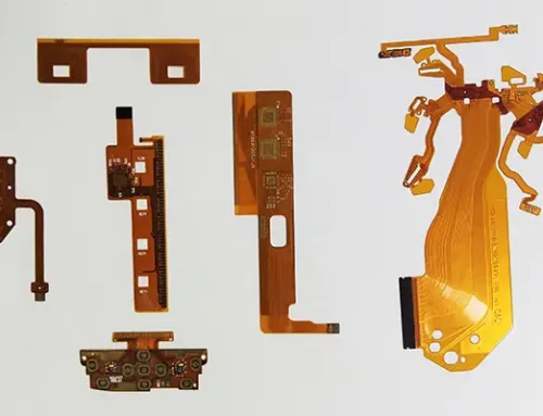
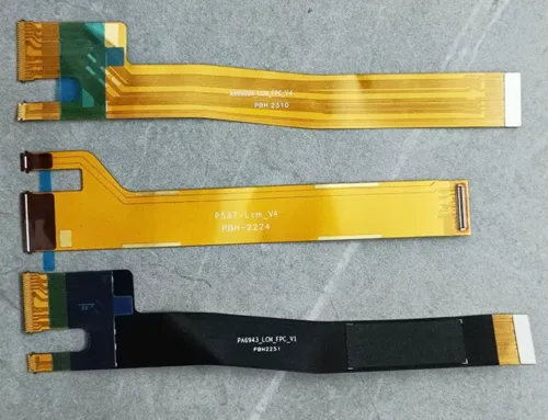
As the “flexible nerves” of electronic devices, the manufacturing of FPC boards represents a precision art in modern industry. In smartphones, FPCs just 0.03mm thick must carry 10A currents; in satellite antennas, multilayer FPCs endure extreme temperature cycles from -180°C to 200°C.
These seemingly contradictory performance metrics are precisely why FPC technology has long been pushed to the limits of materials and processes.
This article dissects the eight core challenges in FPC manufacturing, revealing the “impossible triangle” underlying this technology—the difficult-to-achieve balance between high reliability, ultra-thin structure, and mass producibility.
This remains an engineering conundrum that most companies and engineers strive to solve, yet struggle to fully overcome.
The “Alchemy Dilemma” of Material Systems
The first hurdle in FPC manufacturing lies not in equipment or processes, but in the inherent contradictions within the material system itself. At micron-level thicknesses, every physical parameter of the material is magnified infinitely, where any mismatch translates into risk.
Physical Limits of Substrates
Polyimide (PI) film, the mainstream substrate, faces dual constraints of “performance versus cost,” a contradiction particularly pronounced in high-end FPC applications:
Thermal Expansion Coefficient Mismatch: The difference between PI’s CTE (20×10⁻⁶/K) and copper foil (17×10⁻⁶/K) accumulates internal stress during repeated thermal loading cycles. Production validation shows warpage exceeding 150μm after 100 thermal cycles, posing critical risks for high-density connector soldering and SMT placement.
Dielectric Loss Dilemma: Conventional PI’s dielectric constant (Dk=3.2) struggles to meet 5G millimeter-wave and high-speed signal integrity demands. While modified liquid crystal polymers (LCP) significantly enhance high-frequency performance, their material cost of $800/m² directly limits adoption in consumer electronics.
Thickness Control Cliff: When PI film thickness drops to the 12μm range, material manufacturing and lamination processes enter an “unstable zone.” Even ±1μm thickness variations can cause characteristic impedance deviations exceeding 8%, posing severe challenges for high-speed differential signal links.
From an engineering perspective, PI has approached its physical limits for industrial application. Further performance squeezes must be achieved at the expense of cost and yield.
The Microscopic Battle for Copper Foil
In FPCs, copper foil serves not only as a conductor but also as a core structural component determining bend life and dynamic reliability. Controlling grain orientation in rolled copper foil directly influences dislocation propagation paths and fatigue crack formation mechanisms.

Table 1 Comparison of Bending Life
In high-frequency bending or dynamic applications, nanocrystalline structures can significantly delay crack initiation, but the practical cost is equally steep:
Nanocrystalline copper foil costs five times more than conventional products. Due to its extremely high grain boundary density, it requires specialized etching solutions; otherwise, severe side etching and line width control issues arise.
This underscores that enhancing copper foil performance requires systemic upgrades across the entire manufacturing chain, not isolated breakthroughs.
Quantum Entanglement of Adhesives
Within FPC material systems, adhesives are often underestimated, yet they serve as the “invisible drivers” of stress transfer, thermal aging, and bending endurance. Choosing between adhesive systems fundamentally involves balancing trade-offs across performance dimensions:
Acrylic Adhesive: Exceptional flex resistance (Tg = -40°C) with outstanding performance in dynamic applications, but its upper temperature limit is only 150°C, presenting significant limitations in automotive electronics and high-temperature reflow soldering scenarios.
Epoxy Adhesive: Withstands temperatures exceeding 200°C, but cracks after 50,000 flex cycles under repeated mechanical stress, failing to meet the demands of wearable or foldable devices.
Polyimide adhesive: The latest solution achieves a critical performance balance with a Tg of 180°C and withstands 1 million flex cycles without damage. However, its curing process requires a nitrogen-protected environment, imposing higher demands on production line modifications and cost control.
The selection of adhesives has evolved from a “supporting material decision” to a core engineering decision impacting the long-term reliability of FPCs.
Micron-Level Battle in Precision Manufacturing
The core of FPC manufacturing lies in micron- and even nanometer-level precision control. Any minute deviation can lead to functional failure or yield decline, particularly in high-density interconnections, multilayer stacking, and flexible folding applications.
Nanometer-Level Precision in Graphic Transfer
When employing the Semi-Additive Process (SAP), each step imposes stringent precision requirements:
Copper plating thickness must be controlled within ±0.3μm, which not only determines circuit load capacity but also directly impacts impedance matching and EMI characteristics.
Laser Direct Imaging (LDI) alignment accuracy must be within ±2μm, where any exposure machine temperature drift or optical error is amplified. For instance, one manufacturer scrapped an entire FPC batch due to 0.8μm line width deviation caused by 0.5℃ exposure unit temperature drift.
High-precision pattern transfer demands not only stable equipment but also simultaneous optimization of material thermal expansion coefficients, optical absorption rates, and etch resistance. Otherwise, nanometer-level errors will directly cause high-speed signal chain failure.
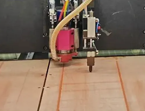
The Plasma Game in Drilling
FPC drilling primarily serves through-holes (vias) and microvia interconnections, with distinct advantages and disadvantages across laser technologies:
CO₂ Laser: Deep penetration, low cost, suitable for thick substrates, but exhibits significant thermal damage to hole walls and irregular microvia morphology.
UV Laser: Features a small spot size, low thermal impact, and precise aperture control, enabling microvias <50μm in diameter. However, equipment investment reaches $3 million per unit, maintenance costs are high, and stringent cleanroom conditions are required.
Engineering often employs a hybrid drilling strategy: CO₂ removal for bulk material followed by UV laser finishing. This balances throughput and precision but demands extremely rigorous process control.

Table 2 Comparison of CO₂ Lasers and UV Lasers
Stress Labyrinth in Multilayer Laminations
In multilayer FPCs, thermal-mechanical property differences between layers generate stacking stresses:
During 8-layer FPC lamination, CTE variations must be controlled within ±2×10⁻⁶/K. Otherwise, warping or delamination occurs during reflow soldering or high-temperature applications.
Interlayer alignment accuracy requires ±5μm; exceeding this range causes impedance mismatch failure. X-ray alignment systems can reduce errors to ±1.5μm, but this reduces production capacity by 40%, illustrating the typical trade-off between precision and throughput.
Plastic flow of materials during lamination, adhesive curing shrinkage, and cumulative thermal expansion must be simulated simultaneously. Otherwise, micron-level errors will inevitably translate into impedance drift or open-circuit risks.
“Ultimate Challenge” of Reliability
FPC reliability transcends material properties, reflecting dynamic performance under multi-physics coupling. Flexure life, solder joint stability, and extreme environment adaptability constitute three critical barriers requiring breakthroughs in design and manufacturing.
Molecular Dynamics of Flexure Life
The relationship between 90° bend radius and failure cycles is as follows:
- R=1mm → 500,000 cycles
- R=3mm → 2,000,000 cycles
- R=5mm → 5 million cycles
However, smartphone hinges demand R=0.5mm with 1 million cycles—exceeding conventional PI and copper foil limits. The solution lies in developing gradient materials: stress buffering and localized reinforcement are achieved through varying copper foil thickness distribution, PI modulus gradients, and adhesive hardness layering.
Additionally, FPC surface coatings, nano-lubricants, and microstructure designs are employed to reduce friction and fatigue crack propagation rates.
Interface Science in Soldering
Soldering is critical for connecting electronic components in FPCs, where high temperatures and metal diffusion impact interface stability:
Lead-free solder (SAC305) application on FPCs is constrained by pad copper thickness:
When pad copper thickness < 5μm, IMC layer growth accelerates by 3x. At peak temperatures of 288°C, PI substrate shrinkage exceeding 0.05% causes solder joint voiding or cracking.
Laser-assisted soldering enables precise local temperature control, maintaining a ±3℃ temperature differential, significantly reducing failures caused by substrate shrinkage. However, the equipment investment reaches $1.2 million, posing a challenge for small and medium-sized production lines.
Additionally, soldering reliability is influenced by multiple factors, including pad surface roughness, solder paste viscosity, reflow profiles, and atmosphere control, forming a classic interfacial science engineering problem.
Environmental Adaptability: The Line Between Life and Death
High-end FPCs, particularly in military and aerospace applications, must withstand extreme environmental challenges:
Temperature Cycling: -65°C to 175°C; insulation resistance > 10GΩ after 500 cycles
Salt Spray Test: 96 hours, corrosion area < 0.1%
Gamma Radiation: Electrical performance degradation < 5% after 50 kGy dose
These metrics conceal complex engineering challenges involving simultaneous control of material interface stability, conductor fatigue, and dielectric aging. No single material optimization can achieve compliance independently; systematic design and stringent process control are essential.
Simultaneously, the accumulation of internal stresses within multilayer FPCs and environmental coupling effects amplify reliability risks stemming from micron-level manufacturing deviations, creating an “extreme battlefield” in FPC production.
“Millimeter-Wave Array” of Cost Control
FPC manufacturing is not only a precision industry but also a high-stakes game of cost control. At the micron level, every millimeter of material, every thermal cycle, and every piece of equipment depreciation directly impacts unit costs.
Material Utilization Dilemma
When processing 600mm-wide PI film, traditional line-based layout achieves only about 65% material utilization, leaving vast amounts of unusable scrap.
Intelligent nesting algorithms can boost utilization to 78%, significantly reducing waste, but their high computational complexity increases processing time.
A real-world case shows that after implementing an AI layout system, a company saved $2 million annually in PI film costs while minimizing human error and cutting losses.
In high-frequency, high-speed FPC production, material utilization not only impacts costs but directly affects micron-level line width consistency and signal integrity. Thus, material layout optimization becomes a critical step before mass production.
The Mathematical Curse of Equipment Depreciation
For a fully automated FPC production line (Table 3), equipment depreciation accounts for 32% of total costs. This means that even with material optimization, equipment depreciation remains an unavoidable fixed cost.

Table 3 Equipment Depreciation
To maintain economic viability, utilization rates must exceed 85%; otherwise, depreciation amortization rapidly erodes profits.
High-precision equipment like LDI imagers, laser drilling machines, and X-ray alignment systems involve significant investment and long depreciation cycles. Production planning must precisely align capacity with order rhythms to prevent “idle running costs.”
Environmental Compliance Cost Cliff
Electroplating wastewater treatment costs represent a significant expense in FPC manufacturing (Table 4), particularly for high-layer and porous structures requiring stringent chemical residue control.
With the EU RoHS 3.0 lowering cadmium limits to 10ppm, testing costs have increased by 30%.

Table 4 Cost Comparison
Companies must balance environmental compliance with cost optimization: efficient wastewater recycling, advanced online detection, and green chemical alternatives have become essential investment directions.
Four Pathways for Technological Breakthroughs
FPC technology is evolving from material limits and process control toward quantum-scale manufacturing and intelligent processes.
Molecular-Level Material Innovation
Graphene-modified PI: Thermal conductivity enhanced to 15 W/m·K, CTE reduced to 12×10⁻⁶/K, significantly improving thermal management and dimensional stability.
MXene conductive ink: Sheet resistance < 0.1 Ω/sq, resistance variation < 2% after 5 million bends, providing reliable support for flexible high-current and foldable applications.
By optimizing material segments through molecular design, FPCs achieve balanced high-frequency performance, bend endurance, and environmental adaptability, fundamentally resolving the “performance-cost-reliability” impossible triangle.
Quantum Manufacturing Technologies
Femtosecond Laser Drilling: Heat-affected zone < 1μm, hole diameter accuracy ± 0.5μm, enabling unprecedented precision control in micro-via interconnects and high-density packaging.
Atomic Layer Deposition (ALD): Deposits 5nm uniform dielectric layers, tripling interlayer dielectric strength and significantly enhancing multi-layer FPC reliability.
New manufacturing technologies shift from traditional mechanical processes to atomic-level control, achieving ultra-high precision and microstructural optimization—the core drivers of next-generation flexible electronics manufacturing.
Intelligent Process Systems
Digital Twin Laminating: Real-time prediction of interlayer stress and warpage trends achieves 98% lamination accuracy, reducing manual trial-and-error and scrap rates.
AI Defect Detection: Missed defect rate < 0.01% with 5x faster detection speed, enabling quality visualization and precision management on high-speed production lines.
These intelligent systems not only boost production capacity and yield rates but also provide technical assurance for industrializing complex FPC designs.
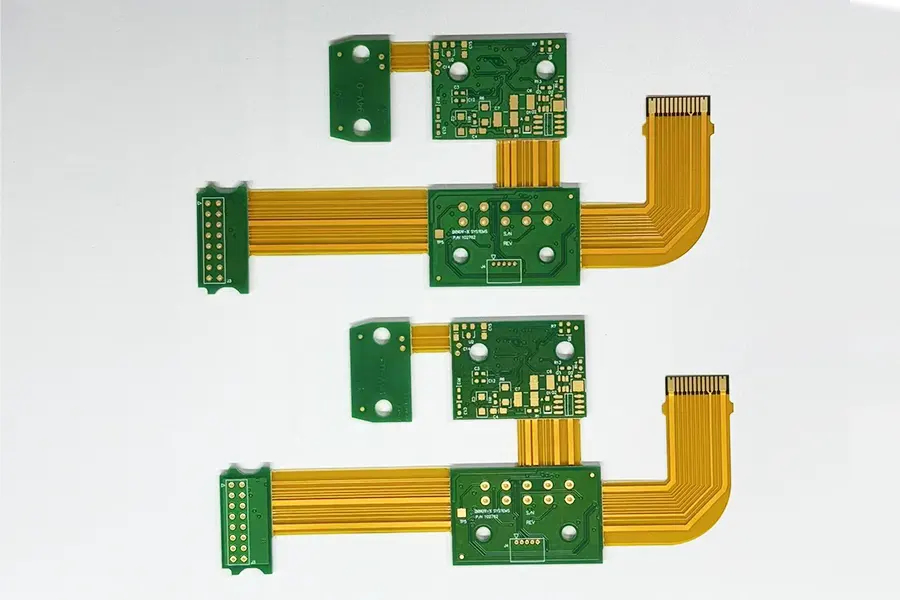
Cross-Dimensional Packaging Revolution
3D-MCM Technology: Integrates up to 10 layers of FPC with an overall thickness < 0.3mm, breaking through 2D layout constraints to achieve high-density, multi-functional integration.
Chip-Embedded FPC: Embeds 0201 components within PI substrates, saving 40% space while reducing interconnect length and signal delay. This delivers unprecedented design freedom for wearables and foldable devices.
Cross-dimensional packaging not only transforms FPC structures but also provides a foundational platform for microsystems, flexible medical devices, and deployable space structures.
Conclusion
FPC manufacturing is undergoing a paradigm shift from “micron-scale engineering” to “quantum manufacturing.”
When line widths break through 3μm, bend cycles reach tens of millions, and costs drop to $0.1/cm², flexible electronics will give rise to new species like implantable medical devices, deployable space structures, and smart wearable terminals.
At the heart of this manufacturing revolution lies the collaborative dance between materials scientists and process engineers at the atomic scale. Through molecular design, quantum processing, and intelligent process systems, they transform physical limits into mass-producible, highly reliable products.
For the entire industry chain, this represents not merely technological advancement but an art of balancing economic efficiency, material utilization, and extreme reliability—heralding the boundless potential of future flexible electronics.