Carbon-Coated Film Evaluation for Reliable FCCL Copper Plating


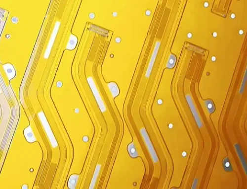
Flexible printed circuits comprise one or more layers of etched conductive material on one or both sides of a dielectric film and are widely used in smartphones, laptops, wearable devices, automotive electronics, and other fields.
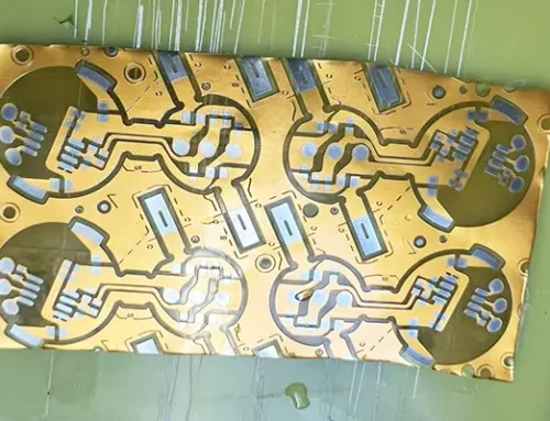
Flexible Copper Clad Laminate (FCCL) serves as the substrate material for flexible printed circuit boards, comprising a flexible insulating base film (typically polyimide, PI) bonded to a metal foil (usually copper).
Role and Challenges of Carbon-Coated Film
Carbon-coated film, a critical step in the via metallization of flexible copper-clad laminates, involves depositing a dense layer of graphite particles with excellent conductivity onto the dielectric layer material of the via walls.
This ensures electrical connectivity between layers within the via, enabling subsequent copper plating to proceed smoothly.
Since the 1980s, carbon-coated film technology has been applied in the production of copper-clad laminates. Variations in process execution directly impact hole quality, making its evaluation crucial for early defect detection.
This prevents waste of labor and resources while avoiding economic losses.
In recent years, to achieve denser film formation and increase particle coverage, the particle size of conductive graphite has progressively decreased. Commercial products now predominantly feature particle sizes in the hundred-nanometer range.
Additionally, the thickness of the graphite layer adsorbed onto the hole walls is extremely thin, typically only tens of nanometers.
In production, it is extremely challenging to rapidly and intuitively observe the adhesion of these nanoscale particles on the substrate.
Currently, no simple and direct method exists to evaluate the effectiveness of carbon plating on flexible copper-clad laminates.
Evaluation Method and Validation Strategy
This paper utilizes the most common flexible copper-clad laminate with PI insulation as a substrate.
Qualitative and quantitative analyses are conducted on the morphology of the film surface and hole walls, contact angles, and electrical resistance to evaluate the effectiveness of the carbon-coated film.
The results are then validated through copper plating tests, ultimately developing a simple and effective method for assessing the performance of carbon-coated films on flexible copper-clad laminates.
Experiments
Primary Materials and Testing Instruments
FRS 522 # SW polyimide film, Tokuyama Corporation, Japan; 2FPDR2003JC flexible copper-clad laminate, Tai Hong Technology Co., Ltd.; Carbon coating process solution, Medeme Technology Co., Ltd.
Sigma500 scanning electron microscope (SEM), Carl Zeiss, Germany; Dimension XR Atomic Force Microscope (AFM), Bruker Corporation, Germany; SL200K CN Contact Angle Tester, Shanghai Solon Information Technology Co., Ltd.; P15V-M(T) Plasma Treatment System, Zhuhai Baofengtang Electronics Technology Co., Ltd.
Sample Preparation and Testing Methods
PI films were cut into 100 mm × 100 mm dimensions and subjected to the carbon coating process steps shown in Figure 1. The films were then removed for microscopic morphology observation.
Subsequently, the PI film underwent plasma etching under carbon tetrafluoride and oxygen conditions, again following the processes in Figure 1, with morphological changes observed.
The surface roughness of the PI film before and after plasma treatment was measured using AFM. Rq denotes the root mean square deviation of the profile, while Rz represents the maximum height of the profile.
To examine hole morphology, a 1 mm diameter hole was mechanically drilled in the FCCL. After carbon coating and plasma etching, the hole was cut open along its diameter from the center, allowing observation of the inner wall morphology from the side.
For scanning electron microscopy (SEM) observation of the PI film and hole walls, gold sputtering was applied to the observation surface to enhance conductivity due to PI’s inherent poor electrical conductivity.
For contact angle measurements, PI film was cut into 30 mm × 10 mm pieces and firmly attached to glass slides with adhesive tape. Contact angles were measured at multiple locations.
For resistance testing, a double-sided FCCL resistance test piece was processed as shown in Fig. 1.
The two terminals of the resistance meter were then clamped onto the copper layers on both sides of the test piece. The resistance measured at this point was recorded as the value after the carbon film deposition process.
Electroplating tests were conducted in a Hall cell. Copper plating was performed for 10 minutes at a current of 1.0 A, and the plating effect on the test piece was observed.

Fig.1 Main process of shadow
Results and Analysis
Morphology of PI Film After Each Carbon Coating Process
Following the carbon coating process, black graphite particles were adsorbed onto the surface of the PI film. The morphological changes of the PI film during the carbon coating process are shown in Figure 2.

Fig.2 SEM images of PI film after each process of shadow
Following pre-microetching and hole-filling agent treatment, no significant changes were observed on the PI film surface (Fig. 2(b), (c)).
After the first shadowing solution treatment, graphite particles were adsorbed onto the PI film surface (Fig. 2(d)), with a particle size of approximately 700 nm.
Following the first fixing solution treatment, some weakly adsorbed graphite particles were rinsed away (Fig. 2(e)).
The trend of graphite particle changes during the second round of hole-opening, shadowing, and fixing processes was similar to that of the first round (Fig. 2(f), (g), (h)).
Ultimately, some areas on the PI film surface were covered by graphite particles, while the remaining exposed regions posed a risk of poor copper plating.
Effects of Plasma Etching on PI Film
Plasma etching is typically performed before carbon film deposition. Figure 3(a) shows the PI film after plasma etching. Compared to the untreated raw material in Figure 2(a), surface pits are visible, and electronegative groups are generated by plasma bombardment.

Fig.3 SEM images of PI film after plasma etching treatment and each process of shadow
Figure 4 shows AFM images of the PI film before and after plasma treatment. The untreated PI film surface is relatively smooth (Fig. 4(a), (b)), while the plasma-treated surface is noticeably rougher (Fig. 4(c), (d)).
The untreated PI film exhibited surface roughness values of Rq = 1.35 nm and Rz = 12.3 nm. After plasma treatment, Rq and Rz increased to 3.37 nm and 27.6 nm, respectively, showing a significant increase compared to the original film.

Fig.4 AFM images of PI film before and after plasma treatment
› Graphite Particle Coverage After Carbon Deposition
Following the first step of hole filling, shadowing, and fixing (Fig. 3(c), (d), (e)), most areas of the PI film surface were covered by graphite particles.
Figure 5 illustrates the coverage extent of particles on the PI film surface, where red indicates areas covered by graphite particles.
Statistical analysis revealed that the coverage rate of the plasma-treated PI film after the first fixing step reached 52.647% (Figure 5(c)), whereas the untreated PI film achieved only 20.690% coverage after the same process (Figure 5(a)).
After the second step of hole alignment, shadowing, and fixing (Figures 3(f), (g), and (h)), the adsorbed graphite particles continued to increase, covering most of the PI film surface.
The particle coverage on the plasma-treated and untreated PI films after the second fix step was 74.182% (Fig. 5(d)) and 46.193% (Fig. 5(b)), respectively.

Fig.5 Particle coverage on the surface of PI film
› Surface Energy and Hydrophilicity Enhancement
The plasma-etched PI film interacts more readily with solvents in the carbon film deposition process compared to the untreated PI film, enhancing its adsorption of graphite particles.
This increased adsorption of graphite particles will facilitate subsequent copper plating processes.
Following plasma etching, the PI film adsorbs more graphite particles after the carbon film deposition process. This phenomenon is also related to changes in the surface hydrophilicity of the film.
Water contact angle measurements reveal that the untreated PI film exhibits an 89° contact angle, which decreases to 35° after plasma etching.
Surface free energy also significantly increases from 29 mN/m for the untreated film to 61 mN/m after plasma etching.
Evidently, the hydrophilicity of the PI film significantly enhances after plasma etching, readily interacting with hydrophilic solvents used in the carbon-coated film process.
This improves surface adhesion, leading to increased graphite particle adsorption.
Hole Wall Morphology
The aforementioned studies demonstrated the changes in standalone PI films during the carbon plating process. A typical flexible double-sided copper-clad laminate consists of two copper foil layers sandwiching a PI layer.
Therefore, in actual production, greater attention is focused on the carbon plating condition on the inner walls of holes after drilling in flexible copper-clad laminates.
The effectiveness of carbon plating on the inner walls is examined qualitatively and quantitatively through microstructure analysis and electrical resistance measurements.
› Hole Wall Microstructure Evolution
Figure 6 presents SEM images of the PI layer on the inner wall of holes in a flexible double-sided copper-clad laminate after mechanical drilling and subsequent carbon plating processes.
It can be observed that after drilling (Figure 6(a)), the PI hole wall layer appears rougher compared to the untreated original film (Figure 2(a)).
Following plasma etching, uniform fine grooves appear on the hole wall (Fig. 6(b)). After the first shadowing and fixing solution treatment (Fig. 6(d), (e)), most areas of the inner hole wall are covered by graphite particles.

Fig.6 SEM images of PI hole wall
› Particle Coverage and Quantitative Analysis
Figure 7 illustrates the particle coverage on the hole walls, where red areas indicate regions where the PI layer is covered by particles.
After the first fixer treatment, particle coverage reached 61.131% (Fig. 7(a)), approaching the coverage achieved in Fig. 5(d) for the PI film after two fixer treatments.
Following the second darkening and fixing solution treatment (Fig. 6(h), (i)), the coverage on the inner hole walls further increased, achieving a particle coverage rate of 98.951% (Fig. 7(b)), significantly exceeding the particle coverage observed on the PI film in Fig. 5(d).

Fig.7 Particle coverage of the hole wall
› Correlation Between Film Surface and Hole Wall Performance
Evidently, the increased roughness of the hole walls after drilling enhances particle adsorption.
The amount of graphite particles adsorbed on the hole walls exceeds that on the planar PI film surface, resulting in complete and dense coverage of the hole walls and excellent performance of the carbon-coated film.
Regarding the adsorption morphology of PI across different carbon-plating processes, the trends observed on the hole walls align with those on the film plane.
Therefore, changes in the film plane can serve as a reference for evaluating material adsorption on hole walls, enabling a preliminary assessment of carbon-plating effectiveness on flexible copper-clad laminate hole walls.
Direct evaluation using the film plane eliminates the drilling process, simplifying and accelerating material handling.
Combined with water contact angle testing to obtain quantitative data, this enables a preliminary assessment of the carbon-coated film’s performance.
Hole Resistance
The aforementioned microstructure clearly and intuitively reveals the adsorption of graphite particles onto the PI dielectric layer of flexible copper-clad laminates, directly reflecting the quality of the carbon-coated film.
Beyond these evaluations, measuring the hole resistance provides a more precise quantitative reflection of the carbon coating’s effectiveness.
The test sample shown in Figure 8 underwent plasma etching. After the carbon coating process—including pre-microetching, first hole alignment, shadowing, and fixing—resistance value A was measured.
Following the second hole alignment, shadowing, and fixing steps, the resistance value B was measured.
The resulting resistance values A and B were 1,457 Ω and 28 Ω, respectively. This indicates that the holes exhibit excellent conductivity and that the carbon coating performs well.
Additionally, the second fix resist value B was lower than the first resist value A, indicating that as the number of carbon film deposition cycles increased, the adsorption of graphite particles increased, leading to a decrease in resist value.
This finding is consistent with the microstructure observed via SEM.
Thus, the effectiveness of the PI carbon-coated film on the dielectric layer of flexible copper-clad laminates was qualitatively and quantitatively evaluated from both microstructure and resistance values, establishing a simple and direct assessment method.

Fig.8 Double-sided FCCL resistance test
Copper Plating Verification
To validate the reliability of the aforementioned method for evaluating carbon film deposition on flexible copper-clad laminates, test specimens, as shown in Figure 9, underwent carbon film deposition and copper plating.
The copper plating condition of the vias was observed to verify the credibility of conclusions drawn from this method.
After plating commences, copper deposition initiates from the bottom, with the lowest holes being filled first, followed by sequential plating of upper holes.
If the preceding carbon film deposition is effective and sufficient graphite particles are adsorbed onto the PI, all holes will be fully plated with copper from bottom to top after 10 minutes of plating.
If the prior carbon coating is ineffective and the PI adsorbs few graphite particles, complete copper plating of the upper holes cannot be guaranteed, particularly those in the upper region of the right-side low-potential area.
After 10 minutes of copper plating at 1.0 A, all 8 holes in both the left-side high-potential and right-side low-potential regions of Figure 9(b) are fully plated with copper.
The cross-section in Fig. 9(c) shows a copper layer deposited on the hole walls within the dashed box.
This indicates that the preceding carbon film deposition was effective, allowing copper to readily deposit onto the graphite particles.

Fig.9 Copper plating test
This conclusion corroborates the findings from Sections 2.3 and 2.4, where hole wall morphology observations and resistance tests demonstrated the excellent performance of the carbon-plated film.
This confirms that the evaluation method for carbon-plated films on flexible copper-clad laminates is reasonable and reliable.
This method enables the prediction of final copper plating outcomes, thereby preemptively eliminating potential copper plating defects and swiftly preventing economic losses.
CONCLUSION
This study investigates the performance of carbon-plated films on typical polyimide-based flexible copper-clad laminates.
It reconstructs the microstructural changes in both the film and the PI pore walls during each carbon-plating process step. It achieves a comprehensive understanding of the carbon-plating mechanism.
Graphite Adsorption and Plasma Enhancement
Graphite particle adsorption occurs after shadowing, with particle diameters approximately 700 nm.
As the number of carbon plating cycles increases, the amount of adsorbed graphite particles also increases.
Following plasma etching, uniform pits appear on the PI film surface, increasing roughness and enhancing adsorption. This leads to more adsorbed graphite particles and improved carbon plating results.
Evaluation Method and Process Validation
Based on this understanding of the carbon film deposition process, an evaluation method for assessing the effectiveness of carbon film deposition on flexible copper-clad laminates was developed.
This method uses microstructure as a qualitative criterion, supplemented by quantitative analysis of water contact angle, surface free energy, and electrical resistance.
Applying this method to both the PI film and the PI layer on the hole walls consistently yielded conclusions of excellent carbon-plating performance.
Electroplating tests demonstrated good copper plating results in the holes, corroborating the aforementioned conclusions and thereby validating the reliability of this evaluation method.
Industrial Application
This method resolves the challenge of observing carbon plating effects during production. It can be applied to evaluate carbon plating performance on FCCL, enabling early screening of optimal raw materials, eliminating the risk of hole breakage, and preventing economic losses.
It also serves as feedback for process parameters such as plasma etching and chemical cleaning, providing a basis for selecting optimal process conditions.