Unlocking the Future of Electronics: How Flexible PCB Buttons Are Changing Device Design


Unlocking the Future of Electronics: How Flexible PCB Buttons Are Changing Device Design
Summary:
Manufacturers create flexible PCB buttons from flexible printed circuit boards. They use very thin copper layers and high-quality dielectric materials. This design allows for slim, high-density PCBs in today’s compact electronic products.
By using advanced flex circuits instead of rigid circuit boards, manufacturers get better durability. This applies to products like remote controls and wearables. They also manage the costs of materials effectively. This guide explores their construction, benefits, design considerations, cost drivers, and future trends.
What Are Flexible PCB Buttons?
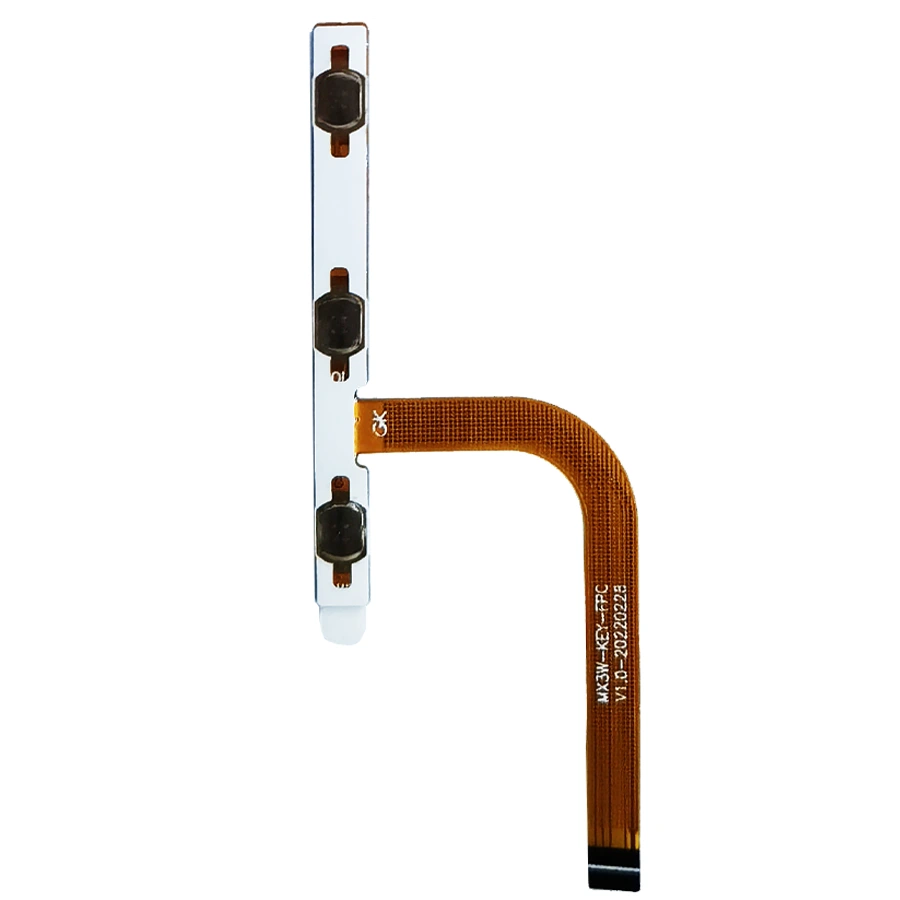
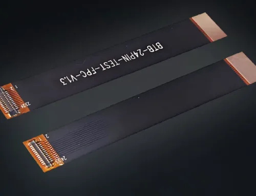
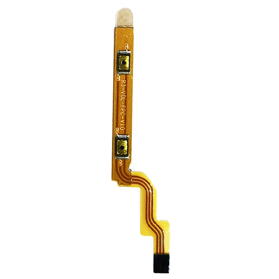
Flexible PCB buttons are switch interfaces made on bendable flex PCBs. They replace wire harnesses and rigid boards in tight spaces.
They consist of etched copper layer traces laminated onto polyimide or polyester dielectric layers, offering both tactile and capacitive actuation
Flex designs can bend repeatedly without breaking. This makes them perfect for side-mounted power and volume keys, as well as main control buttons.
Key Components & Materials
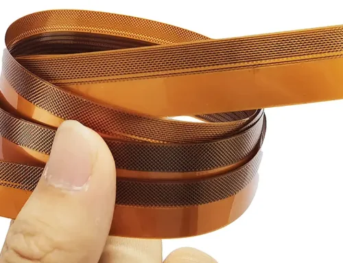
Copper Layer: Ultra‑thin copper foil (as low as 9 µm) delivers high conductivity in high-density layouts
Dielectric Materials: Polyimide and polyester substrates provide electrical insulation and flex endurance. Multi‑layer stacks balance signal integrity and flexibility
Dielectric Layers: Thin dielectric films between copper traces prevent crosstalk and maintain performance in compact button arrays
Expensive Materials: While polyimide and fine‑pitch copper raise material costs, they enable miniaturization and reliability that rigid boards cannot match
Design & PCB Layout Considerations
When integrating flex circuits into PCB design, engineers must:
Optimize Trace Routing: Use high-density interconnect (HDI) methods to place micro-vias and narrow traces. This maximizes routing in small button areas
Layer Selection
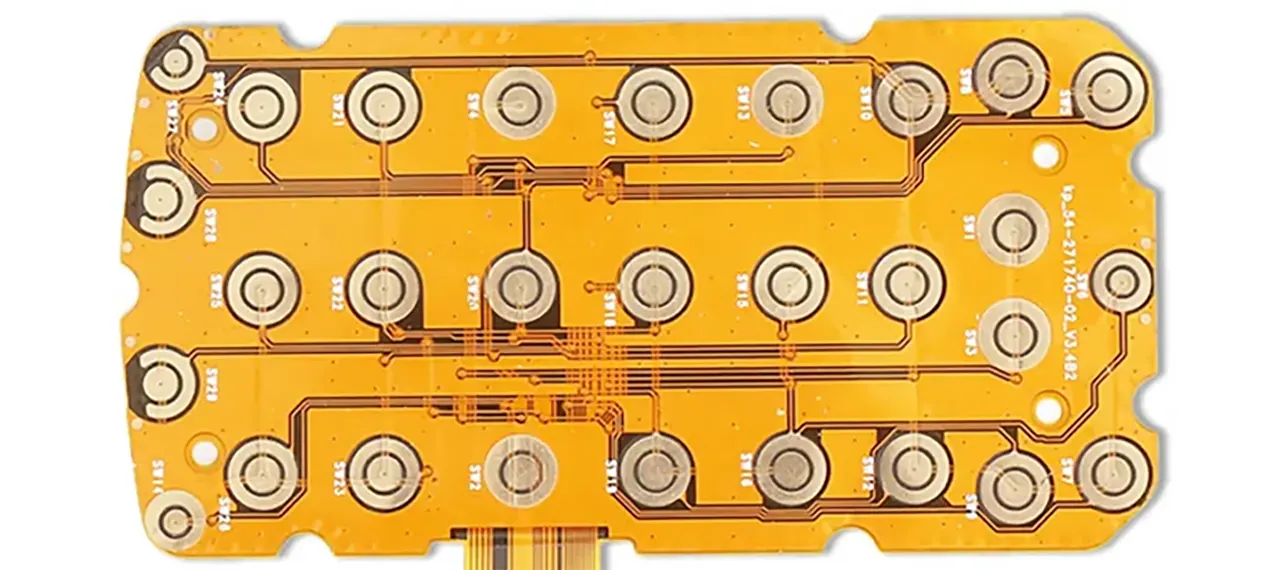
- You can choose a single-layer flex for simple switch matrices.
- Alternatively, you can select multi-layer structures for complex button arrays and sensor integration
Rigid‑Flex Transitions: Incorporate stiffeners or rigidized zones to anchor the button area, balancing flexibility with mechanical support
Material Stack‑up: Select dielectric thickness and copper weight to achieve target impedance, signal integrity, and tactile response
Applications in Electronic Products
Flexible PCB buttons appear across diverse devices:
Remote Controls: Slim handheld units leverage flex circuits for multi‑button layouts, reducing assembly complexity
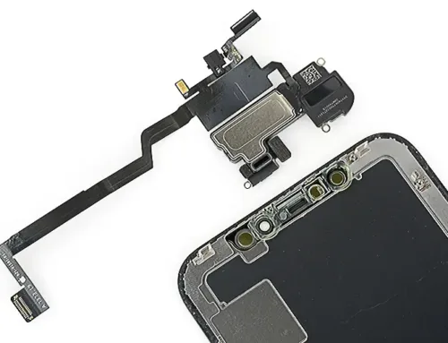
Wearable Electronics: Smartwatches and fitness bands use flex PCBs to fit buttons within curved housings without bulky wiring
Automotive Controls: Dashboard and steering‑wheel buttons demand durability under temperature extremes—flex designs meet these harsh environmental requirements
Advantages Over Rigid Circuit Boards
Cost Optimization
The initial material costs are higher. However, savings from assembly and fewer errors can lower total ownership costs. This reduction can be up to 70% compared to wire harnesses
Key Features of Flexible PCB for Buttons
- Ultra-Thin and Lightweight
Flexible PCBs are designed to be super-thin, with a thickness of less than 0.1mm. This is why they work well for ultra-thin devices like smartphones, tablets, and wearables, where space and weight matter.
- Flexibility and Durability
With these PCBs, devices with frequent button usage will receive consistent performance even after repeated bending and dynamic movements. They are especially suitable for foldable devices or gadgets with complex mechanical layouts. - Stable Signal Transmission
Flexible PCBs help send signals from a power button or a main keypad. They ensure low signal loss and quick response times. This guarantees smooth functionality across all button types. - Customizable Designs
Flexible PCBs can be customized to fit various button configurations, including single-layer and multi-layer designs. Manufacturers can tailor the PCB layout to meet specific product requirements, ensuring optimal performance and integration.
Future Trends
Check out similar products on Amazon
FAQ:
Flexible PCB buttons are switch interfaces built on bendable flexible printed circuit boards. They use thin copper traces laminated onto polyimide or polyester substrates to create tactile or capacitive button functions. Their bendability allows them to fit into compact or curved device housings while maintaining reliable electrical performance.
Flexible PCB buttons offer major advantages over rigid boards, including:
Up to 30% reduction in device thickness and weight
Higher durability under repeated bending and button presses
More reliable signal transmission for fast and accurate response
Support for complex button layouts in tight spaces
These benefits make flex buttons ideal for smartphones, wearables, automotive controls, and slim consumer electronics.
Key materials include:
Ultra-thin copper foil (as low as 9 µm) for fine-pitch signal routing
Polyimide or polyester dielectric layers for insulation and flex endurance
Dielectric films to prevent crosstalk in dense button arrays
Although some materials like polyimide are more expensive, they offer superior durability, heat resistance, and miniaturization capabilities.
Engineers must consider:
Trace routing with HDI methods such as micro-vias and narrow traces
Single-layer vs. multi-layer stack-ups depending on button complexity
Rigid-flex transitions using stiffeners for mechanical stability
Material stack-up choices that affect impedance, tactile feel, and signal integrity
These design decisions ensure the flex button performs reliably under mechanical stress.
Flexible PCB buttons are widely used in:
Remote controls for slim multi-button panels
Wearables like smartwatches and fitness trackers
Automotive controls requiring high durability under temperature extremes
Consumer electronics, including smartphones and gaming controllers
Their ability to bend, fold, and fit into small enclosures makes them ideal for modern compact devices.
Major cost drivers include:
Copper thickness and precision (fine-pitch HDI designs increase cost)
Substrate type, with polyimide costing more than FR-4
Production volume, where large batches reduce per-unit pricing
Surface finishing and testing, such as ENIG coatings and automated bend tests
Although material costs can be higher, total system costs may drop by up to 70% compared to wire harness assemblies.