Optimizing Blind Slot Multilayer Flexible PCB Manufacturing: A New Laser-Controlled Fabrication Method


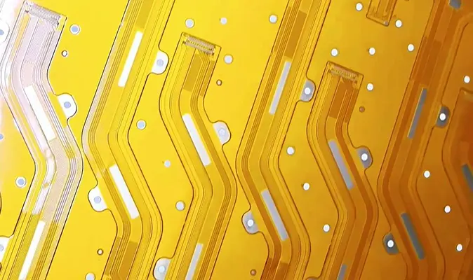
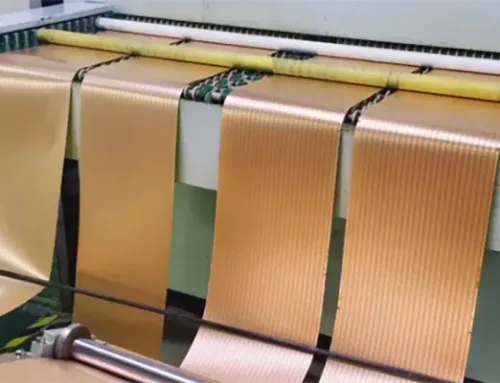
As an interconnection between electronic components, multilayer flexible printed circuit boards (FPCBs) meet the circuit connection needs of various electrical and electronic products. They align with the industry trend toward lighter, thinner, shorter, smaller, higher-performance, and high-density electronic devices.
Electronic products become increasingly miniaturized and diversified. Traditional planar circuit boards face significant constraints in space utilization and safety. Fail to meet evolving demands.
Consequently, blind slot circuit boards have emerged. Flexible printed circuits inherently possess the advantage of bendability over rigid printed circuits.
Blind slot multilayer flexible printed circuits better satisfy high-density mounting requirements, leading to growing applications in aerospace, aviation, and military sectors in recent years.
This paper presents a new process method for blind slot machining in multilayer flexible printed circuits, using a 12-layer flexible PCB with blind slot design as an example. It aims to provide valuable insights for the fabrication of such products.
Product Information and Process Design
Basic Product Information
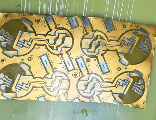
This product is a 12-layer flexible printed circuit board with a stackup as shown in Figure 1. The CS-L4 and SS-L7 layers feature blind vias, exposing patterns on L4 and L7, respectively.
L4 and L7 traces carry signal transmission requirements and receive thin gold plating. The blind vias on the CS-L7 layer serve as signal shielding holes. Traces on the CS and SS layers receive thick gold plating.

Figure 1: Product Stack-up Diagram
Current Manufacturing Process
L4-L5 Process: Material Cutting → Internal Exposure → Punching → Inner Layer Etching Inspection → External Exposure → Thin Gold Plating → External Exposure (exposing only conductors, dry film covering conductors by 0.079 mm) → Alkaline Etching (etching conductors) → Standard Process.

L4 L5 Process
Pure Resin Process: Material Cutting → Trimming (Pure resin window near blind slot bottom is 0.127 mm larger than slot on one side) → Auxiliary Material Matching.
CS-L7 Process: Laminating → Copper Reduction → Drilling → Plasma Treatment → Copper Plating → Internal Exposure → Acid Etching → Outer Layer Etching Inspection → External Exposure 1 → Thin Gold Plating → Alkaline Etching (Film Removal Only, No Etching) → Outer layer imaging 2 → Alkaline etching 1 (etching conductors) → Outer layer etching inspection 1 → Assembly center → Brown passivation.

CS L7 Process
CS-SS Process: Laminating → Drilling → Plasma treatment → Copper plating → Outer layer imaging → Acid etching → Outer layer etching inspection → Outer layer imaging 1 → Thick gold plating → Alkaline etching (film removal only, no etching) → Outer layer imaging 2 → Alkaline etching 1 (etch conductors) → Outer layer etch inspection 1 → Laser milling of blind vias (laser depth-controlled opening) → Normal process.

CS SS Process
Shortcomings of the Manufacturing Process
The primary approach in the current process for producing blind vias in multilayer flexible boards involves creating a pure adhesive window near the bottom of the blind via.
After lamination forms the CS-SS layer, the flexible cover above the blind via is milled through using laser depth control (e.g., for a 12-layer flexible PCB, milling through the CS-L1, L2-L3 core layers, and the pure resin layer between core layers).
The milled cover is then peeled off to form the blind slot and expose the pattern at the bottom. The critical control point in this method lies in adjusting the laser energy.
It must ensure sufficient power to mill through the blind slot cover without damaging the circuitry at the bottom of the blind slot.
Whether using CO₂ laser processing or UV laser processing, the material is heated, melted, and vaporized by laser energy.
Processing inconsistencies in laser energy intensity can lead to uneven cutting depths and challenges in controlling the residual thickness of the cover.
Therefore, the process of creating blind vias in multilayer flexible printed circuits by directly laser-controlled depth milling through the flexible layer cover presents challenges:
Either excessive cutting depth may damage the blind via pattern, or insufficient depth may result in incomplete PI penetration, causing cover tearing during removal.
Improvement Section
Improvement Proposal
Identify shortcomings in the existing process for fabricating blind vias in multilayer flexible printed circuits. The current method uses direct laser-controlled depth milling. This method penetrates the flexible cover layer to form the blind vias.
Propose a novel method for fabricating blind vias in multilayer flexible printed circuits.
The flexible core layer near the bottom of the blind via is first laser-milled along the blind via outline. During lamination, a PI protective tape is applied over the blind via location.
Block adhesive with the tape. Provide partial protection for the internal circuit patterns within the blind via. Prevent direct damage to these patterns caused by laser alignment errors or uneven energy distribution during milling.
During laser cover removal, only the topmost flexible cover layer is cut to a controlled depth, avoiding milling into the flexible core layer adjacent to the blind slot. The optimized laminate structure is illustrated in Figure 2.

Figure 2: Protect the bottom of the blind groove with tape.
The optimized and improved manufacturing process is as follows:
L2-3, L8-9 Process Flow: Material Cutting → Internal Photolithography → Punching → Inner Layer Etching Inspection → Laser Milling (along blind slot edges) → Center Alignment → Brown Coating.
L4-L5 Process: Material cutting → Internal photolithography → Punching → Inner layer etching inspection → External photolithography → Thin gold plating → External photolithography (exposing only conductors, dry film covering conductors by 0.076 mm) → Alkaline etching (etching conductors) → Center alignment → Brown oxidation → Applying PI protective tape.
CS-L7 Process: Laminate → Copper Reduction → Drilling → Plasma Treatment → Electroplating Copper → Internal Exposure → Acid Etching → Outer Layer Etch Inspection → External Exposure 1 → Thin Gold Plating → Alkaline Etching (Film Removal Only, No Etching) → External Exposure 2 → Alkaline Etching 1 (wire etching) → Outer layer etch inspection 1 → Component placement → Brown passivation → Apply PI protective tape.
Pure Resin Process: Material cutting → Trimming (pure resin near blind via bottoms requires no windowing, only vent hole trimming) → Component placement. The remaining processes remain unchanged.
Improvement Results
Following the improvement plan, laser windows were pre-cut in the core board near the blind vias before lamination. The product boards were remanufactured with protective tape applied over the blind vias.
Inspect the blind via circuit appearance and PI quality on the blind via sidewalls of the improved finished product. Show no defects, such as laser milling damage to the blind via circuit or delamination caused by PI peeling during cover removal.
Table 1 records the defect rate comparison before and after the improvement. The optimized results demonstrate significant effectiveness, substantially enhancing the product yield rate (see Table 1).
| Status | Laser Milling Blind-Groove Profile Defect Rate | PI Cover Layer Delamination Defect Rate | Blind-Groove Residual Adhesive Defect Rate | Total Defect Rate |
|---|---|---|---|---|
| Before improvement | 25 pcs / 200 pcs = 12.5% | 13 pcs / 200 pcs = 6.5% | 0 pcs / 200 pcs = 0% | 19% |
| After improvement | 0 pcs / 200 pcs = 0% | 0 pcs / 200 pcs = 0% | 0 pcs / 200 pcs = 0% | 0% |
Conclusion
(1) Fabricate blind vias in multilayer flexible printed circuit boards by directly performing laser-controlled deep milling through the flexible layer cover. Risk laser milling damage to the blind via pattern or failure to fully cut through the PI layer during lid separation due to uneven laser energy distribution.
(2) Apply PI protective tape to the blind slot bottom. Cut through the flexible core board adjacent to the blind slot before lamination. Effectively mitigate laser damage to blind slot patterns and lid separation issues. Ensure suitability for producing blind slots in multilayer flexible printed circuits.