Flexible Tactile Sensor Design Using FPCB Processing for Robotic and Industrial Applications


Tactile sensors can obtain relevant characteristics of both the sensor and the contacted object’s surface through physical contact, such as temperature, pressure, hardness, and material properties. With the advancement of robotic bionics, the application scope of these “artificial skin”-like tactile sensors continues to expand, playing an increasingly vital role in robotic bionics, medical devices, and various industrial equipment.
Scholars have conducted extensive research on tactile sensors, employing diverse designs. Lee et al. from the University of Minnesota utilized polydimethylsiloxane (PDMS) as the structural material to develop a capacitive tactile sensor.
This sensor offers advantages such as high flexibility and sensitivity, though it has a limited measurement range. In subsequent research, they encapsulated four tactile units together, supported by a central cylindrical pillar, enabling shear force measurement.
Additionally, common approaches for tactile sensors include piezoelectric and fiber optic types. Extensive research indicates that flexible tactile sensors predominantly utilize polymeric materials such as PDMS, polyvinylidene fluoride (PVDF), polyimide (PI), and conductive rubber.
However, processing these materials often requires MEMS fabrication techniques, which involve cumbersome steps, high costs, extended lead times, and compromised yield rates. Building upon the operating principles of capacitive tactile sensors, a flexible tactile sensor structure based on distributed capacitance was designed. It was fabricated using FPCB processing, which offers low cost, short lead times, high yield rates, and facilitates mass production.
Experiments demonstrate that the FPCB-processed tactile sensor can detect forces applied to its sensing surface. By controlling FPCB processing parameters and the thickness of the spacer layer, the sensor’s sensitivity, linearity, and measurement range can be adjusted.
Principle and Structural Design of the Sensor
Figure 1 shows the schematic diagram of the flexible tactile sensor proposed in this paper. For illustrative purposes, only one tactile cell is depicted.
The upper electrode and lower electrode are embedded in the upper electrode layer and lower electrode layer respectively, separated by an intermediate spacer layer. This configuration forms a capacitor between the two electrodes, constituting a tactile unit.
When an external force acts upon the contact point above the tactile cell, the distance between the upper and lower electrodes changes, causing a variation in the capacitance value of that cell. By detecting this capacitance change using a dedicated signal detection circuit, the magnitude of the force applied to the contact point can be calculated.

Fig. 1 Schematic diagram of sensel without a shield
To shield against external electromagnetic interference and minimize the impact of surface charges on the measured object, another FPCB structure with a shielding layer was designed for experimentation. This structure features a fully copper-filled and grounded top layer on the upper electrode layer FPCB, as illustrated in Figure 2.

Fig. 2 Schematic diagram of sensel with a shield
Array Configuration and Signal Acquisition
In the proposed tactile sensor, the tactile elements are arranged in an array configuration. To simplify wiring, the upper and lower electrodes are shared. The capacitive surface array signal of the entire tactile sensor is read out in an array-like manner through the detection circuit. This signal is transmitted in real-time to the host computer.
After processing, the force distribution across the entire upper surface of the tactile sensor can be determined. The tactile units of the designed sensor form an 8 × 8 array with a spatial resolution of 5.08 mm and an effective detection area of approximately 9 cm × 9 cm.
Fabrication and Assembly of the Tactile Sensor
The proposed tactile sensor adopts a “sandwich” structure, primarily composed of three laminated layers: an upper electrode layer, a lower electrode layer, and an intermediate spacer layer.
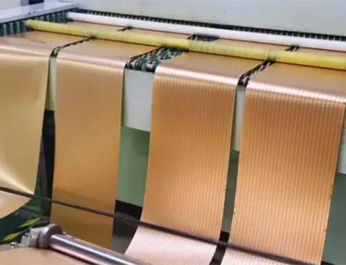
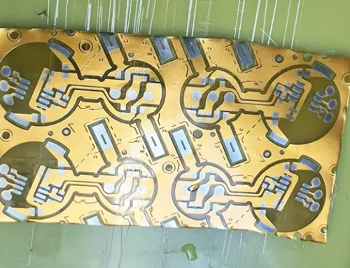
Both the upper and lower electrode layers are fabricated using FPCB technology, with the upper electrode traces routed on the bottom layer of the upper electrode layer and the lower electrode traces on the top layer of the lower electrode layer. Figure 3 shows the finished upper and lower electrode layers after processing.
The intermediate spacer layer is made of silicone rubber. Rectangular cavities are etched at the positions corresponding to the upper and lower electrodes of each contact point. This design maximizes the deformation of the upper electrode layer under contact force, thereby enhancing the sensor’s sensitivity.
A circular silicone block is affixed directly above each contact point as the sensing surface. This further increases sensitivity while protecting the sensor’s upper surface from scratches when exposed to foreign objects.

Fig.3 Photos of fabricated FPCB
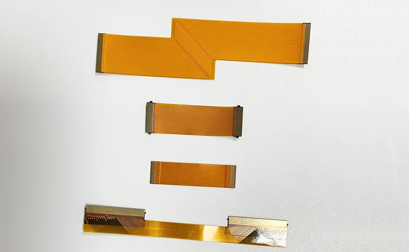
To facilitate detection of the sensor’s capacitive signals, the upper and lower electrodes of the sensor are routed to the same side of the sensor via leads within the FPCB.
The signals are then transmitted to the signal detection circuit through the FPCB connection lines. Figure 4 shows the finished sensor product, demonstrating that the designed tactile sensor exhibits excellent flexibility.

Fig. 4 Photo of the designed tactile sensor
Experiment
Figure 5 shows the experimental setup for the calibration test. For ease of calibration, the designed flexible tactile sensor rested on a horizontal acrylic plate.
The push-pull force gauge remained secured to a vertical guide rail, with its probe positioned directly above the contact point. A precise micro-motion platform controlled the magnitude of vertical displacement to apply a specific normal force.

Fig. 5 Experiment apparatus of calibration
Sensor Calibration Experiment
Engineers fabricated three distinct FPCB types as the upper and lower electrode layers for the proposed tactile sensor: a 100 μm thick unshielded FPCB, a 200 μm thick unshielded FPCB, and a 200 μm thick shielded FPCB.
The spacer layer thickness also varied across three parameters: 200 μm, 300 μm, and 400 μm.
Based on the different FPCB structures and spacer layer thicknesses, a total of nine tactile sensors underwent fabrication.
Calibration experiments then investigated the relationship between FPCB structure, spacer layer thickness, and performance metrics such as measurement range and sensitivity.
Each sensor underwent three experiments, with results analyzed for measurement range, sensitivity, linearity, and repeatability.
Results for 100 μm Thick Unshielded FPCB
Figure 6 shows experimental results using an FPCB with a 100μm thick unshielded layer.

Fig. 6 Experiment results of 100 upm thick FPCB without shield layer
Table 1 shows the relevant characteristics of the tactile sensor on an FPCB with a 100 μm-thick unshielded electrode layer.
| 200 μm Thickness | 300 μm Thickness | 400 μm Thickness | |
|---|---|---|---|
| Measurement Range / N | 2 | 9.5 | 9.5 |
| Sensitivity (% / N) | 25.19 | 14.38 | 10.85 |
| Linearity Error (%) | 4.49 | 7.97 | 8.74 |
| Repeatability Error (%) | 7.44 | 5.00 | 4.61 |
As shown in Figure 6(a), when the spacer layer thickness is 200 μm, the sensor’s sensitivity curve shifts significantly downward when the force applied to the sensor’s sensing plane exceeds 2 N, indicating sensor overload.
To ensure good linearity and service life, we specify its measurement range as 2 N.
For spacer thicknesses of 300 μm and 400 μm, the measurement range is 9.5 N. As shown in Figures 6(b) and 6(c), the sensitivity curve exhibits good linearity within the 9.5 N range.
We therefore define its measurement range as 9.5 N. As shown in Table 1, when testing tactile sensors on FPCBs with a 100 μm electrode layer and no shielding layer, increasing the spacer layer thickness results in a larger measurement range but reduced sensitivity, while simultaneously decreasing repeatability error.
When the spacer layer thickness is 200 μm, the sensor’s range is significantly affected by overload linearity, making it suitable for applications requiring high sensitivity but low range.
Compared to a 400 μm spacer layer, a 300 μm spacer layer provides higher sensor sensitivity and smaller linearity error, but slightly poorer repeatability.
Results for 200 μm Thick Unshielded FPCB
Figure 7 shows the experimental results using a 200 μm thick FPCB without a shielding layer.

Fig. 7 Experiment results of 200 μm thick FPCB without shield layer
Table 2 shows the relevant characteristics of the tactile sensor on an FPCB with a 200 μm-thick unshielded electrode layer.
| 200 μm Thickness | 300 μm Thickness | 400 μm Thickness | |
|---|---|---|---|
| Measurement Range / N | 3 | 9.5 | 9.5 |
| Sensitivity (% / N) | 21.88 | 6.09 | 3.82 |
| Linearity Error (%) | 7.59 | 8.09 | 8.26 |
| Repeatability Error (%) | 4.31 | 5.72 | 3.88 |
As shown in Figure 7(a), when the spacer layer thickness is 200 μm, the slope of the sensor’s output sensitivity curve changes significantly when the applied force exceeds 3N, approaching overload.
To ensure good linearity and service life, the sensor’s measurement range is specified as 3 N at this point. For spacer thicknesses of 300 μm and 400 μm, the measurement range is 9.5 N.
As shown in Table 2, overall, the sensor’s sensitivity decreases with increasing spacer thickness.
At 200 μm spacer thickness, the sensor exhibits a smaller measurement range but higher sensitivity; while at 300 μm and 400 μm, the sensor exhibits higher sensitivity at the former thickness but slightly larger repeatability error, with linearity error remaining comparable.
Results for 200 μm Thick Shielded FPCB
Figure 8 presents experimental results using a 200 μm thick shielded FPCB.

Fig. 8 Experiment results of 200 μm thick FPCB without shield layer
Table 3 shows the relevant characteristic parameters of the tactile sensor employing a 200 μm thick shielded FPCB as the electrode layer.
| 200 μm Thickness | 300 μm Thickness | 400 μm Thickness | |
|---|---|---|---|
| Measurement Range / N | 9.5 | 9.5 | 9.5 |
| Sensitivity (% / N) | 5.83 | 2.34 | 2.42 |
| Linearity Error (%) | 7.77 | 4.88 | 12.24 |
| Repeatability Error (%) | 2.83 | 5.60 | 7.89 |
Due to the copper layer deposited on the top electrode layer, which increases its hardness, the sensitivity of the shielded design decreases significantly compared to the unshielded design, as shown in Table 3.
However, observations on the host computer reveal that the tactile sensor with this design exhibits markedly reduced noise when contacting the test object. The shielded tactile sensor suits applications where high sensitivity isn’t needed but noise sensitivity matters.
These nine sets of experiments lead to the conclusion that as the spacer layer thickness increases, the sensor sensitivity decreases.
However, when the spacer layer thickness is 200 μm, the sensor sensitivity significantly improves compared to a 300 μm spacer layer. Under identical spacer layer thickness conditions, thicker and stiffer FPCBs exhibit lower sensitivity.
Demonstrate through experiments that designing different FPCB structures and spacer thicknesses enables development of tactile sensors with varying sensitivity, measurement ranges, and other specifications to meet diverse application requirements.
Sensor Array Experiment
Figure 9 (left) shows a colored pen cap inverted over the surface of the designed tactile sensor, with a finger applying light pressure.
Figure 9 (right) displays the grayscale image processed by the host computer. Comparing Figure 9 (left), the points with lower grayscale values correspond to the sensor elements pressed by the pen cap’s edge.
Areas not pressed by the cap show minimal grayscale variation, indicating that the designed sensor elements accurately detected pressure applied to the sensing surface.

Fig. 9 Experiment of a pen cap
Figure 10 (left) shows a standard tennis ball placed on the surface of the designed tactile sensor and pressed slightly.
The contact point at the bottom of the ball experiences the greatest force, while the surrounding contact points experience slightly less force. The contact elements not pressed by the ball remain unaffected.
The array detection results are shown in Figure 10 (right). The gray values at the contact point directly beneath the tennis ball are noticeably higher, while those along the outer edge show a slight decrease. Gray values at the unexposed areas remain largely unchanged.
The detection results align well with the actual conditions, indicating that the designed tactile sensor accurately detected the force distribution between the tennis ball and the sensor’s sensitive surface.

Fig. 10 Experiment of tennis
Array scanning experiments of the sensor demonstrated that the designed tactile sensor can detect tactile force signals on the sensor surface and visualize these signals on the host computer.
Conclusion
These tests examined the relationship between the sensor’s range, sensitivity, and other metrics with these parameters. 400 μm.
These experiments explored the relationship between the designed tactile sensor’s range, sensitivity, and other metrics with these two parameters.
Experiments demonstrated that thicker FPCBs exhibit greater rigidity, while larger spacer thicknesses result in reduced tactile sensor sensitivity and increased measurement range.
Selecting these parameters allows designing tactile sensors with distinct characteristics to meet diverse application requirements.
Array scanning tests confirmed that the designed tactile sensor can capture surface force signals, enabling “artificial skin”-like functionality. This provides a novel design approach for robotic skin and tactile diagnosis applications.