What is the Class-Wire Harness Flexible PCB Manufacturing Technology?


In recent years, the rapid development of high-end industries such as intelligent connected vehicles and low-altitude aircraft has driven continuous innovation in flexible printed circuit boards (FPCBs).
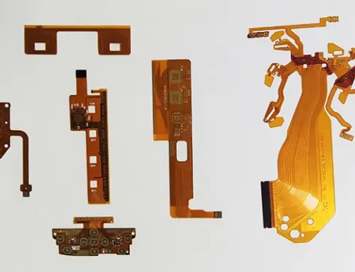
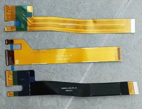
In traditional automotive applications, certain wiring and distribution functions rely on wire harnesses, as illustrated in Figure 1. Conventional wire harnesses feature a structure where copper wires are encased in plastic insulation material.
Multiple strands of wiring are bundled together and wrapped in insulating material to form a single harness.
During actual operation, each harness must connect to an electrode. When multiple current signals are present, numerous harnesses often work in tandem. This inevitably increases the space occupied within the vehicle, placing higher demands on spatial layout.

Figure 1: Traditional wire harness
Compared to traditional wiring harnesses, FPCBs offer advantages such as a more organized layout, a more compact structure, reduced space requirements, superior safety performance, lighter weight, greater manufacturing flexibility, and the ability to support automated production and assembly.
Consequently, numerous FPCB products have emerged in recent years to replace traditional wiring harnesses.
Initially, FPCBs were primarily used to replace wiring harnesses in battery packs, enhancing both safety and energy density.
As the technology advanced, its advantages expanded its application scope into fields like smart connected vehicles, extending to modules such as intelligent control and human-machine interaction.
However, these new applications also imposed fresh demands on FPCB design, manufacturing, and performance.
This paper focuses on the FPCB used in a certain brand’s smart connected vehicle battery pack. It innovatively derives new structural design concepts from a manufacturing perspective, subsequently developing unique processing methods to successfully create a new product.
Application Scenario Analysis
The customer specified requirements for this FPCB: it must fit within a compact space with a width distribution constrained to 5 mm or less.
The board must accommodate numerous conductive and signal traces while maintaining impedance accuracy within ±10%.
Additionally, since the connection application involves non-unidirectional bending, this FPCB is used at the interface between horizontally and vertically mounted modules, as shown in Figure 2.
Therefore, the FPCB must possess non-parallel bending performance to meet customer requirements.

Figure 2: FPCB connection module structure in a non-single parallel direction
Novel Design and Processing Method
Novel Structural Design
Considering the aforementioned application scenario, the following factors were comprehensively evaluated:
(1) Due to constraints imposed by the connected module dimensions, a multi-layer FPCB structure design is not feasible.
(2) The FPCB must exhibit non-parallel bending performance.
(3) While maintaining FPCB performance, prioritize manufacturing process simplicity and enhanced cost-effectiveness.
(4) The FPCB must additionally provide impedance control and withstand repeated flexing cycles.
Following in-depth discussions with the client and considering all design constraints, it was decided to approach the structural design from a manufacturing perspective.
This involved reverse-engineering and optimizing the application-oriented structure by thoroughly examining the FPCB design from a manufacturing standpoint.
Research led to the adoption of a redesigned layout forming a single-sided or double-sided FPCB with a rectangular outline measuring 20mm × 130mm.
The FPCB features an integrated structure at both ends, with multiple sub-FPCBs in the central section. These sub-FPCBs undergo lamination after forming, resulting in an FPCB with integral ends and a multi-layer laminated structure in the middle.
Novel Structural Design
Following confirmation of the design structure, key processing steps were outlined as shown in Table 1.
| Key Process | Description |
|---|---|
| Layout Redesign | Design the FPCB as a planar structure of “two end regions + central region.” The two end regions each serve as integrated connection terminals. The central region consists of multiple sub-boards arranged in parallel and evenly distributed. Gaps are formed between sub-boards along the length direction as processing areas, reserved for subsequent cutting. For example, if the total width is 15 mm and divided into 3 sub-boards, each sub-board width is 5 mm. |
| Front-End Process | Material cutting, patterning, coverlay lamination, etc. |
| Manufacture Single-Sided or Double-Sided FPCB | Manufacture the FPCB using standard conventional methods, and fabricate stacked winding guide lines on the FPCB. |
| Fabricate Individual Sub-Boards | Use die punching or laser cutting processes to cut the gap processing areas, forming individual sub-boards. |
| Winding Process | Stack the sub-boards and use winding adhesive tape to wind according to the stacked winding guide lines. |
| Post-Process | Inspection, packaging, etc. |
Table 1 Key FPCB Processing Steps
Further research into processing methods identified the following critical technical points:
(1) Local sub-board processing and anti-tear technology for laminated layers.
(2) Selection of winding materials and winding processing techniques.
(3) Impedance stability technology.
Breakthroughs in these key technologies will highlight the technical characteristics of this novel structural product and provide robust support for establishing a complete, operational processing workflow.
Key Technology Analysis and Implementation
Local Sub-Board Processing and Anti-Tear Laminating Technology
During development, single- or double-sided FPCBs formed through manufacturing are extremely thin, measuring only 0.12 mm ± 0.03 mm.
Laser cutting or die-cutting techniques are employed to directly create “slits” in the central region of the FPCB, forming the sub-board structures.
This process presented two major challenges:
On one hand, since the end regions of the FPCB are interconnected as a single unit, when sub-boards in the central laminated area intersect during lamination, significant internal stress is generated within the board body.
This stress readily causes tearing at both ends of the slits.
On the other hand, during mass production using die-cutting technology, the retracting cutting tool may pull on both ends of the “slot” during the retraction process, similarly causing board tearing.
To address these issues, a solution was developed: adding “anti-tear holes” at both ends of the processed “slot.” Specifically, before creating the “slot,” through-holes with diameters of 0.15–0.50 mm are pre-drilled at both ends of each pattern.
This technique leverages the stress-relieving or buffering effect of the through-holes during lamination to prevent panel tearing.
Second, the “slit” was redesigned as a “through-slot.” The width was expanded from 0 mm to 0.2–0.8 mm, forming a slot after processing.
Punching the “slot” using a die provides stress relief during retraction, preventing tearing of the 2024 No.12 flexible and rigid-flex printed circuit boards (FPCB and R-PCB) during retraction. See Table 1.
Further research on processing methods is required, with key technical points as follows:
(1) Local sub-board processing and laminate tear-resistant technology.
(2) Selection of winding materials and winding processing technology.
(3) Impedance stability technology.
Breakthroughs in these key technologies will highlight the technical characteristics of this novel structural product and strongly support the establishment of a complete, operational processing workflow.
Key Technology Analysis and Implementation
Local Sub-Panel Processing and Laminate Anti-Tear Technology
During development, single- or double-sided FPCBs were fabricated with extremely thin thicknesses of 0.12 mm ± 0.03 mm.
Laser cutting or die-cutting techniques were employed to directly create “slits” in the central region of the FPCB, forming the sub-panel structures.
Challenges in Sub-Panel Processing
This process presented two major challenges:
First, since the end regions of the FPCB are interconnected as a single unit, when sub-boards in the central laminated area meet at the interface, significant internal stress is generated within the board body.
This stress readily causes tearing at both ends of the slit.
Second, during mass production using die-cutting technology, the retraction of the cutting tool during the die-back process may pull on both ends of the “slit,” similarly leading to board tearing.
Anti-Tear Solutions
To address these issues, the first solution involves adding “anti-tear holes” at both ends of the processed “slot.” Specifically, before creating the “slot,” through-holes with diameters of 0.15–0.50 mm are pre-drilled at both ends of each pattern.
This technique leverages the stress-relieving or stress-buffering effect of the through-holes during lamination to prevent board tearing.
Second, the “slot” was redesigned as a “through-slot.” This involved widening the slot from 0 mm to 0.2–0.8 mm, creating a channel-like structure after processing.
Punching the “through-slot” with a die provides stress buffering during retraction, preventing tearing caused by retraction forces.
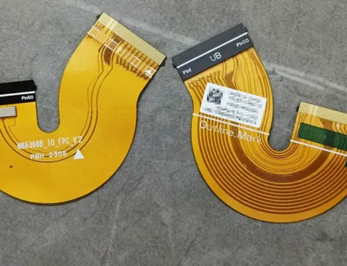
Simultaneously, during lamination of sub-boards, the “through-slot” buffers internal stresses at both ends, further preventing panel tearing during the lamination process. The designed tear-resistant holes and punched “through-slot” structure are shown in Figure 3.

Figure 3: Tear resistant hole and through slot structure plate
Advanced Wire Harness-Like FPCB Considerations
For certain advanced wire harness-like flexible circuit boards with higher requirements and more stringent application conditions, merely incorporating tear-resistant holes may still lead to panel tearing during sub-panel stacking or subsequent insertion/soldering operations, as illustrated in Figure 4.

Figure 4: Tear hole indicates a problem with the plate.
Enhanced Tear-Resistant Hole Process
To address the aforementioned issues, this study further developed a new process.
During the fabrication of single- or double-sided FPCBs, tear-resistant holes are formed along with hole rings.
Depending on application requirements, the single-side width of the hole ring is set between 50 and 300 μm.
For double-sided FPCBs, during the plating process, tear-resistant holes are simultaneously plated to form double-sided hole rings.
During subsequent cover film lamination, windows are first cut in the film at the hole ring locations before application, ensuring the rings remain exposed after lamination.
The copper layer of the hole rings provides enhanced strength and toughness, significantly reducing the risk of substrate tearing during lamination. The improved flat structure of the wire-like FPCB is shown in Figure 5.

Figure 5: Improved FPCB planar structure for wire harness
Selection of Winding Materials and Winding Processing Technology
The FPCB formed via the above process comprises multiple sub-boards. These sub-boards can be further laminated to create a localized laminated wire-like structure.
Laminating Materials and Process
Special laminating materials are required during the lamination process. Since the cover film layer of the FPCB itself carries an acrylic adhesive or epoxy resin adhesive layer, acrylic adhesive or epoxy resin adhesive is typically considered for the laminating adhesive.
The process is completed through the steps of “adhesive layer preparation → lamination → localized pressing.”
Screen printing and semi-curing baking techniques are employed to create the liquid adhesive layer, but this process requires numerous auxiliary tools.
Additionally, since the cover film is made of polyimide material with high inertness, it must first undergo plasma treatment to create a rough surface, further enhancing the bond strength between the adhesive layer and the cover film.
This results in process complexities, high costs, and low yield rates.
Process Challenges and Improvements
Since the laminating process involves non-planar layering, localized compression must be applied to the “central region” after stacking.
This necessitates creating specialized compression molds to ensure precise positioning, which increases costs and complicates the workflow.
Regarding processing quality, using acrylic or epoxy adhesives for laminated compression often leads to edge adhesive overflow issues.
Removing overflow using laser ablation not only adds further steps and costs but also carries the risk of incomplete ablation.
Wire Harness-Like Structure Development
Based on the application scenarios and environments provided by the customer, combined with the structural patterns of traditional wire harnesses, an improved wire harness-like flexible circuit board was developed.
After laminating the sub-boards, this circuit board employs tape wrapping to form a wire harness structure in the central region, while the end regions feature flat mating and soldering surfaces.
Several tapes supporting this design were tested and compared with acrylic or epoxy adhesives. The material with optimal performance is shown in Table 2.
| Item | Acetate Cloth Tape | 3M Tape | Insulating Tape | Acrylic Adhesive | Epoxy Resin Adhesive |
|---|---|---|---|---|---|
Main Material | Acetate cloth composite methyl methacrylate adhesive | Polyphenyl methacrylate adhesive | Polyethylene | Acrylic ester, methyl methacrylate copolymers | Epoxy resin |
High-Temperature Resistance / °C | −40 ~ 150 | −40 ~ 120 | 0 ~ 80 | −40 ~ 150 | −50 ~ 150 |
Corrosion Resistance | Resistant to water, oil, acid, alkali, mold, chemical corrosion | Resistant to water, oil, acid, mold | Resistant to water, acid, mold | Resistant to water, oil, acid, alkali, mold, chemical corrosion | Resistant to water, oil, acid, alkali, mold, chemical corrosion |
Adhesion Strength | Approx. 3.0 N / 25 mm | Approx. 5.0 N / 25 mm | Approx. 2.0 N / 25 mm | Approx. 7.5 N / 25 mm | Approx. 7.5 N / 25 mm |
Service Life / a | >15 | >15 | >10 | >15 | >15 |
Relative Cost | Lower | Higher | Lower | Higher | Higher |
Environmental Performance | Excellent | Average | Average | Average | Average |
Application Technology Requirement | Winding type, relatively simple | Winding type, relatively simple | Winding type, relatively simple | Screen printing or coating type, relatively complex | Screen printing or coating type, relatively complex |
Post-Application Reliability | Firm adhesion, not prone to bubbling | Firm adhesion, not prone to bubbling | Moderate adhesion, prone to bubbling in long-term use | Firm adhesion, not prone to bubbling | Firm adhesion, not prone to bubbling |
Table 2: Performance Comparison of Different Materials
Table 2 indicates that acetate cloth tape offers superior overall performance.
Its inherent flexibility and breathability provide excellent bendability, effectively preventing issues like inadequate heat dissipation during FPCB operation.
Wrapping the sub-board with acetate cloth tape requires no additional tools.
Engineers complete processing by following the “stacking → wrapping” sequence, forming a robust adhesive bond and securing fixation in the stacked area. Additionally, acetate cloth meets most FPCB wrapping requirements.
Figure 6 shows the structure after the engineers performed localized stacked wrapping. For applications demanding higher reliability, acrylic or epoxy adhesives remain viable alternatives.

Figure 6: Improved FPCB-like wire harness structure after partial layering and winding
Through comparative validation, engineers recommend using 0.15 mm thick acetate cloth tape during the manufacturing process of this FPCB product.
The tape width should match the length of the wrapping area (i.e., the distance between the guide lines on both sides of the wrapping zone).
Wrapping 2 to 4 turns ensures good adhesion and restraint, guaranteeing the FPCB’s excellent flexibility.
Impedance Stability Technology
Following the aforementioned process flow, engineers produced an improved wire harness-like FPCB with localized layering and flat ends. As required, the product must exhibit an impedance of (100 ± 10) Ω.
During testing and application, engineers evaluated the impedance of the non-stacked, unwound planar FPCB.
Results confirmed the product’s impedance capability. However, stacking caused mutual interference between impedance lines across sub-boards, resulting in unstable impedance values exceeding specifications.
To address these issues, further research proposed the following measures:
(1) First, apply shielding film to the laminated area of the board, then create gaps or through-slots.
Alternatively, after forming the laminated structure in the laminated area, apply a shielding film to the surfaces of each sub-board located below, then complete the local lamination and wrapping process.
Verification shows this method effectively mitigates excessive and unstable impedance values, controlling impedance within the range of (100±5) Ω.
Engineers may use conventional electromagnetic shielding film or conductive adhesive film. Figure 7 shows the planar structure with the locally applied shielding film.

Figure 7: Planar structure of FPCB with partial shielding film attached
(2) Follow the procedure in Method (1), but replace the shielding film with acetate cloth.
Acetate cloth itself lacks shielding properties, but verification shows that applying it enhances separation between layers in the laminated region, thereby reducing signal interference between layers.
Compared to shielding film, acetate cloth is lower in cost and maintains material consistency with the acetate cloth used in subsequent winding processes.
This avoids processing complexities and significant performance variations caused by using multiple materials.
This approach effectively addresses excessive impedance issues, controlling values within the (100±10) Ω range.
(3) Cover both sides of the circuit layer with shielding copper layers.
This solution operates on the same principle as applying shielding film.
The copper layer can be designed as a mesh pattern to enhance the FPCB’s flexibility, with the cross-sectional structure shown in Figure 8.
This approach has been verified to effectively mitigate excessive and unstable impedance values, maintaining them within the range of (100±5) Ω.
However, this approach requires designing the FPCB as a multilayer structure, increasing manufacturing complexity, difficulty, and cost.
It is suitable when the board demands high structural integrity and precise impedance control.

Figure 8: Cross-sectional structure of FPCB with added shielding copper layer design
Product Outcomes
Finished Product Appearance
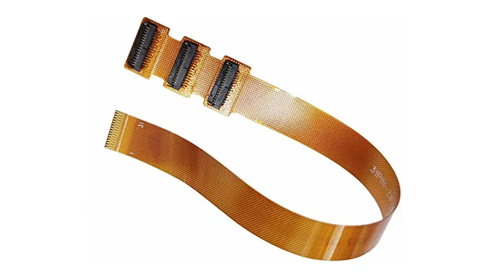
Through innovation and breakthroughs in key technologies, the team successfully manufactured eight improved wire harness-like FPCB products. Figure 9 shows a representative product.

Figure 9: Appearance of the improved wire harness FPC product.
Test Results
| No. | Test Item | Measurement Result | Conclusion |
|---|---|---|---|
| 1 | Bending Resistance ① | 180° bending for 200,000 cycles, resistance change rate is 0.03% (less than ±10%), no circuit breakage | Pass |
| 2 | Bending Resistance ② | Side-direction 180° bending for 100,000 cycles, resistance change rate is 0.03% (less than ±10%), no circuit breakage | Pass |
| 3 | Impedance Test | Differential impedance value is (100 ± 10) Ω, no mutual interference, no excessive fluctuation or other defects observed | Pass |
| 4 | Insulation Resistance | 1.4 × 10¹² Ω (meets the receiving-state requirement of not less than 500 MΩ) | Pass |
| 5 | FPCB Thickness / mm | 0.12 ± 0.03 | Pass |
| 6 | Thermal Stress Test | Test conditions set to 260 °C, 10 s, 3 cycles; no board blistering, white spots, discoloration, or other defects observed; no acetic cloth delamination or bubbling; no layer separation observed on cross-section | Pass |
Table 3: Test Methods and Compliance Standards for Performance Metrics
Conclusions
Addressing the customer’s specialized FPCB application requirements, this project pioneered a novel approach of reverse-engineering design solutions from a manufacturing perspective.
This enabled the effective design of an improved wire-like FPCB structure featuring localized laminated winding, alongside the establishment of an integrated manufacturing process.
During R&D, key innovations and breakthroughs in critical technologies included:
(1) For localized sub-board processing and laminate tear resistance, engineers added anti-tear holes and redesigned the “gaps” as “through slots.”
For higher-demand products, engineers implemented anti-tear holes with annular structures to ensure laminate and winding processing quality, preventing board tearing during application.
(2) After evaluation, engineers selected 0.15 mm thick acetate cloth as the material and applied winding technology to process the central laminated area of the FPCB, wrapping it 2 to 4 turns.
This solution provides strong adhesion and restraint, enabling the FPCB to exhibit excellent flexural properties.
(3) To enhance impedance stability, apply shielding film or acetate cloth to the laminated area of the board.
Alternatively, cover both the top and bottom circuit layers with shielding copper layers.