How to Quick-turn flex PCB prototyping?


In electronic product development, speed is no longer a secondary optimization—it has become a core competitive parameter.
Across wearables, medical electronics, IoT devices, and consumer products, design teams are operating under compressed development cycles where electrical validation, mechanical integration, and regulatory milestones overlap rather than occur sequentially.
Why Quick-Turn Flex PCB Prototyping Is Now a Competitive Requirement
Market data reflects this shift. According to industry surveys, hardware development cycles in consumer and IoT electronics have shortened by 30–50% over the past decade, driven by faster SoC iteration, aggressive launch schedules, and increased product differentiation pressure.
In this environment, flex PCBs—once treated as specialty interconnects—are now central to product architecture, particularly where space constraints, dynamic motion, or complex 3D packaging are involved.
Traditional flex PCB manufacturing lead times, often exceeding 3–5 weeks, fail to support modern development workflows.
When electrical teams wait weeks for first-article validation, mechanical and firmware teams are forced into parallel assumptions, increasing the likelihood of late-stage rework.
The real-world consequences are measurable: missed launch windows, delayed regulatory submissions, and significantly higher redesign costs once tooling and enclosure designs are locked.

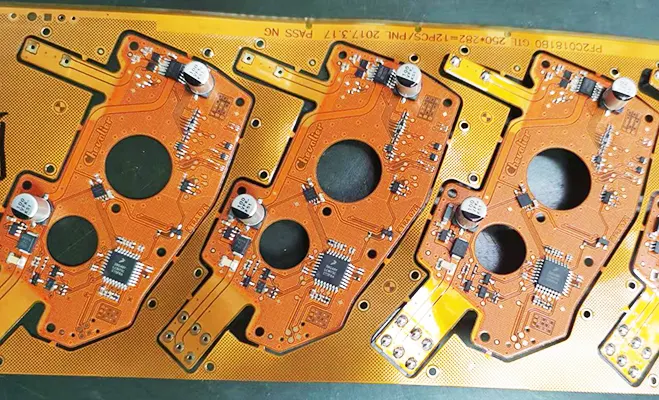
rapid Flex pcb
Quick-turn flex PCB prototyping addresses this bottleneck directly.
Quick-turn flex PCB prototyping is the accelerated fabrication of functional flexible printed circuit prototypes—typically within days rather than weeks—to enable rapid electrical, mechanical, and reliability validation before production release.
For engineering teams under time pressure, the ability to obtain a fast flex PCB prototype is no longer a convenience—it is a prerequisite for maintaining schedule integrity.
What “Quick-Turn” Really Means in Flex PCB Prototyping (Not Marketing Claims)
The term “quick-turn” is widely used but poorly defined across the PCB industry. Many suppliers apply it as a marketing label rather than a process classification, leading to unrealistic expectations among design teams.
In practice, turnaround time is determined by material availability, layer count, process complexity, and inspection requirements.
A clear distinction between standard, quick-turn, and rush services is essential for accurate planning.
Comparison of Flex PCB Turnaround Categories
| Service Type | Typical Lead Time | Manufacturing Characteristics | Risk Profile |
|---|---|---|---|
| Standard Flex Prototype | 15–25 working days | Full material options, conservative process flow | Lowest |
| Quick-Turn Flex | 5–10 working days | Limited stack-ups, expedited CAM & lamination | Moderate |
| Rush Flex | 3–5 working days | Process compression, tight DFM margins | Elevated |
| Super-Rush | 24–72 hours | Highly constrained designs only | High |
Lead time also varies significantly by board architecture. Based on typical factory capabilities:
| Flex PCB Type | Realistic Prototype Time |
|---|---|
| 1–2 Layer Flex | 3–5 working days |
| 4–6 Layer Flex | 7–10 working days |
| Rigid-Flex Prototype | 10–15 working days |
Unlike rigid PCBs, flex circuits require additional steps—polyimide handling, coverlay lamination, controlled impedance under bending conditions, and more complex yield management. These steps limit how far timelines can be compressed without sacrificing reliability.
Claims such as “24-hour flex PCB” are only realistic under narrow conditions: single-layer designs, standard materials, no impedance control, no dynamic bend zones, and waived cosmetic or reliability inspections. For most functional prototypes, such timelines are the exception, not the rule.
Understanding fast turn flex PCB lead time realistically allows engineers to plan validation phases without relying on optimistic assumptions.
When You Should (and Should NOT) Use Quick-Turn Flex PCB Prototyping
Quick-turn flex PCB prototyping is a powerful tool—but only when applied at the right stage of development. Using it indiscriminately can increase cost without improving outcomes.
Quick-turn fabrication delivers the highest value during EVT and early DVT, when electrical functionality, signal integrity, and mechanical behavior must be validated before design freeze.
It is especially effective for verifying bend radius compliance, connector alignment, impedance behavior in flex zones, and thermal performance in compact assemblies.
Engineering teams preparing demo units for trade shows, investor presentations, or clinical evaluations also benefit from accelerated availability.
Conversely, quick-turn should be avoided when designs are not DFM-ready. Incomplete stack-ups, undefined bend zones, or unresolved material selections often lead to CAM holds or scrap—negating any schedule advantage.
Designs requiring exotic dielectrics, specialty copper alloys, or heavy HDI structures rarely fit accelerated workflows. Likewise, quick-turn is not suitable for volume builds; per-unit cost increases sharply as quantities rise.
By clearly defining when speed adds value—and when it does not—engineering teams maintain credibility while controlling risk.
Flex PCB Types That Are Best Suited for Quick-Turn Prototyping
Not all flex PCB architectures respond equally well to accelerated manufacturing. Matching design intent to manufacturability is essential.
Single-sided flex circuits are the fastest and lowest-risk option. With minimal lamination steps and straightforward inspection, they are ideal for sensor tails, button interfaces, and low-density interconnects.
Double-sided flex PCBs offer the best balance between routing density and turnaround speed. They support controlled impedance and moderate component integration while remaining compatible with most quick-turn process flows.
Multilayer flex designs introduce complexity through sequential lamination, registration control, and yield sensitivity. While quick-turn is possible, lead times extend and design discipline becomes critical.
Rigid-flex prototypes require realistic expectations. The combination of rigid core processing and flex lamination inherently limits speed. Even in optimized workflows, rigid-flex quick-turn prototypes typically require at least two weeks to maintain structural and electrical integrity.
Chip-on-Board (COB) flex circuits are rarely compatible with true quick-turn schedules. Bare die attachment, underfill curing, and reliability screening impose fixed process durations that cannot be safely compressed.
Understanding these distinctions enables engineers to select flex PCB prototype types aligned with both schedule and risk tolerance.
Design Rules That Directly Control Flex PCB Prototype Speed
For flex PCBs, design decisions translate directly into manufacturing time. Engineers who understand this relationship can eliminate days—or even weeks—from prototype cycles.
Stack-Up Choices That Save Days
Adhesiveless polyimide constructions consistently yield faster approval and higher reliability than adhesive-based stacks.
They reduce thickness variation, improve thermal stability, and simplify lamination control. Standard copper weights—particularly 0.5 oz—are processed more quickly than heavier foils and are sufficient for most signal and low-power applications.
Unnecessary layers increase lamination cycles and inspection steps; minimizing layer count is the most effective way to reduce lead time.
Bend Area Design for Fast Approval
Bend zones are the first area manufacturers evaluate during DFM review.
Minimum bend radius increases with layer count; as a rule of thumb, single-layer flex can tolerate a radius of 6–10× material thickness, while multilayer flex often requires 12–20×.
Static and dynamic flex zones must be clearly distinguished in documentation. Ambiguity here is a common cause of design rejection or clarification delays.
Routing Rules That Prevent Re-Spins
Trace orientation in bend areas should follow the bend axis whenever possible to reduce strain concentration.
Vias are typically prohibited in dynamic flex zones and tightly restricted even in static bends.
Staggered routing distributes stress more evenly than stacked routing, while curved traces outperform sharp angles in both fatigue life and manufacturability.
These practices reduce the likelihood of CAM modifications and re-spins—critical for maintaining a fast prototype cycle.
Collectively, these principles define flex PCB design for quick turn and directly influence approval speed, yield, and reliability.
Materials That Enable (or Kill) Quick-Turn Flex PCB Prototypes
In quick-turn flex PCB prototyping, material selection is often the dominant factor determining whether a design can be fabricated in days—or stalled for weeks.
Unlike rigid PCBs, flex circuits rely on a narrower ecosystem of qualified materials, many of which are not universally stocked.
Polyimide Films: Stocked Thicknesses Matter
Most quick-turn flex PCB lines are optimized around a limited range of polyimide (PI) film thicknesses. Commonly stocked options include 12.5 μm (0.5 mil), 25 μm (1 mil), and 50 μm (2 mil).
These thicknesses support the majority of single- and double-layer flex designs while maintaining predictable bending performance.
Non-standard PI thicknesses, even when technically viable, often require special sourcing and incoming inspection, immediately adding days to the schedule.
From a speed perspective, selecting a stocked PI thickness is one of the simplest ways to preserve a fast prototype cycle.
Copper Foil Types and Availability
Copper selection influences both electrical performance and manufacturability.
Rolled annealed (RA) copper is preferred for dynamic flex applications due to its superior fatigue resistance, while electrodeposited (ED) copper is more common in static flex or cost-sensitive designs.
However, RA copper is typically stocked only in standard weights—most commonly 0.5 oz and 1 oz. Requests for unusual copper weights or specialty alloys frequently shift the project out of quick-turn eligibility.
Engineers aiming for fast flex PCB prototypes should align current-carrying requirements with these readily available options whenever possible.
FCCL: In-Stock vs Special Order
Flexible copper clad laminate (FCCL) availability is a decisive factor in turnaround time. Manufacturers with in-house FCCL inventory can begin processing immediately, while special-order materials introduce uncontrollable delays.
| FCCL Type | Typical Availability | Impact on Lead Time |
|---|---|---|
| Standard PI + RA Cu | In stock | No delay |
| Adhesive-based FCCL | Limited stock | +2–3 days |
| High-Tg / specialty PI | Special order | +7–14 days |
Competitor articles often describe material properties but rarely address inventory reality. In practice, in-stock FCCL is what enables true quick-turn flex PCB prototyping.
Coverlay vs LPI: Speed Implications
Coverlay remains the dominant protection method for flex circuits, but it adds lamination and curing steps. Liquid Photoimageable (LPI) solder mask, when permitted by design and reliability requirements, can shorten processing time by eliminating coverlay tooling.
That said, LPI is not universally suitable—particularly in dynamic flex zones or high-bend applications. Engineers should view LPI as a speed optimization option rather than a default replacement.
Stiffeners: Not All Materials Are Equal
Stiffeners improve component support and assembly reliability, but material choice directly affects lead time.
| Stiffener Material | Availability | Quick-Turn Compatibility |
|---|---|---|
| FR-4 | Widely stocked | Excellent |
| Polyimide | Stocked (limited thickness) | Good |
| Stainless steel | Special order | Poor |
FR-4 stiffeners are by far the fastest option and are compatible with most quick-turn schedules. Stainless steel stiffeners, while mechanically advantageous, are one of the most common causes of prototype delays.
File Preparation Checklist for Fast Flex PCB Prototyping
For quick-turn flex PCB prototypes, file completeness is as critical as design correctness. Even a manufacturable design can lose days due to preventable documentation gaps.
Required Files: The Zero-Delay Package
A complete flex PCB prototype package includes manufacturing data that clearly communicates mechanical intent—not just electrical connectivity.
In addition to standard Gerber or ODB++ outputs and separated PTH/NPTH drill files, manufacturers require a stack-up drawing that specifies materials and thicknesses unambiguously.
Equally important is explicit bend zone definition. Flex regions, rigid regions, and any dynamic bend areas must be clearly marked. Stiffener drawings should indicate material, thickness, location, and attachment method.
Where controlled impedance is required, impedance notes must reference trace geometry and target values rather than relying on assumptions.
Providing this information upfront enables CAM engineers to proceed without clarification loops.
Common File Mistakes That Add 2–5 Days
The most frequent causes of delay are not electrical errors, but omissions. Missing coverlay layers, undefined flex zones, or ambiguous tolerances force manufacturers to pause fabrication while seeking confirmation.
Incomplete fabrication notes—particularly regarding material substitutions—can also halt quick-turn workflows.
For teams searching for flex PCB prototype files or a flex PCB Gerber checklist, the underlying principle is simple: every unanswered question costs time.
Realistic Cost Expectations for Quick-Turn Flex PCB Prototypes
Speed in flex PCB fabrication carries a measurable premium, and engineers evaluating suppliers should understand where that cost originates.
Typical Cost Multipliers by Lead Time
| Lead Time | Relative Cost |
|---|---|
| Standard prototype | 1.0× |
| Quick-turn (5–10 days) | 1.5–2.0× |
| Rush (3–5 days) | 2.5–3.5× |
| Super-rush | 4.0×+ |
Flex PCB premiums are inherently higher than rigid PCB premiums because flex fabrication involves lower yields, more manual handling, and tighter material constraints. Unlike rigid boards, flex panels cannot always be pooled efficiently, increasing per-unit cost.
Hidden Costs Engineers Often Miss
Beyond the quoted fabrication price, quick-turn flex prototypes absorb additional costs in engineering time, material scrap from accelerated processing, and expedited logistics. These factors explain why flex PCB pricing scales nonlinearly with speed.
Reducing Cost Without Slowing Delivery
Cost control does not require sacrificing lead time. Using in-stock materials, minimizing layer count, avoiding unnecessary stiffeners, and submitting DFM-ready files all reduce internal risk for the manufacturer—often translating into lower pricing even on quick-turn orders.
How to Choose the Right Quick-Turn Flex PCB Prototype Manufacturer
Not all PCB suppliers offering “quick-turn flex” operate true flex manufacturing lines. Selecting the right partner is a technical decision, not a branding exercise.
Must-Have Capabilities
A credible quick-turn flex PCB manufacturer operates a dedicated flex production line, not a repurposed rigid line.
In-house FCCL inventory is essential for schedule reliability. Equally important is access to CAM engineers experienced specifically in flex design, capable of providing actionable DFM feedback within 24 hours.
Critical Questions to Ask Before Ordering
Before releasing files, engineers should verify whether quoted lead times refer to fabrication completion or ship date.
Asking what materials are physically in stock today often reveals more than any datasheet. Clarifying how DFM issues are handled—and how many similar flex prototypes the supplier has successfully built—helps separate experienced manufacturers from intermediaries.
For engineering teams, these questions reduce risk. For capable suppliers, they demonstrate technical confidence rather than salesmanship.
Typical Quick-Turn Flex PCB Prototype Timeline (Day-by-Day)
One reason many engineering teams struggle to plan flex PCB prototypes is the lack of process transparency.
Competitors often quote lead times without explaining where the time actually goes. In reality, quick-turn flex PCB prototyping follows a tightly coupled sequence where delays in any step propagate immediately.
A Realistic 6-Day Quick-Turn Flex PCB Timeline
| Day | Process Stage | Engineering Reality |
|---|---|---|
| Day 0 | File submission & DFM review | CAM checks stack-up, bend zones, materials, drill strategy; most delays originate here |
| Day 1–2 | Material preparation & imaging | FCCL cutting, inner-layer imaging, registration control |
| Day 3–4 | Lamination & drilling | Coverlay/lamination cycles and controlled drilling dominate schedule |
| Day 5 | Coverlay opening & surface finish | Alignment accuracy directly affects yield |
| Day 6 | Electrical test & shipment | 100% continuity test is mandatory for flex |
This visibility is critical for project managers and lead engineers aligning electrical validation with mechanical and firmware milestones. True quick-turn capability is not about skipping steps—it is about compressing transitions between steps without compromising reliability.
Common Failures in Fast Flex PCB Prototyping—and How to Avoid Them
Accelerated schedules increase exposure to failure modes that are less common in rigid PCBs. Understanding these risks allows engineers to design proactively rather than reactively.
Cracked copper in bend zones is the most frequent failure in fast flex prototypes. It typically results from tight bend radii combined with ED copper or traces routed perpendicular to the bend axis. Using RA copper and curved trace routing significantly reduces strain concentration.
Pad lifting often occurs near stiffener transitions, where localized stress combines with thermal cycling during reflow. Enlarging pad fillets and maintaining gradual stiffness transitions mitigates this risk.
Coverlay misalignment is a common side effect of rushed lamination when tolerances are not clearly defined. Explicit coverlay opening dimensions and alignment notes reduce ambiguity during tooling.
Unexpected impedance drift arises when accelerated processing alters dielectric thickness or copper geometry. This is especially critical for high-speed flex interconnects. Specifying impedance targets with acceptable tolerance ranges—not single-point values—improves first-pass success.
Mechanical mismatch with the enclosure is frequently traced back to missing or unclear bend zone definitions. Flex PCBs are mechanical components as much as electrical ones; unclear mechanical intent almost guarantees rework.
These issues dominate search queries related to flex PCB prototype failure and flex PCB bending problems, yet they are rarely addressed directly by suppliers.
Quick-Turn Flex PCB Prototyping FAQs (High-Traffic Section)
- How fast can flex PCB prototypes really be made?
For simple 1–2 layer flex designs using in-stock materials, functional prototypes can be fabricated in 3–5 working days. More complex multilayer or rigid-flex designs typically require 7–15 days even under quick-turn conditions. - Is 24-hour flex PCB manufacturing real?
Only under very limited conditions: single-layer flex, standard FCCL, no coverlay complexity, no impedance control, and waived cosmetic requirements. It is not realistic for most engineering validation builds. - Can rigid-flex prototypes be quick-turn?
Yes, but expectations must be realistic. Rigid-flex quick-turn prototypes generally require 10–15 working days due to sequential lamination and combined rigid/flex processing steps. - What is the minimum order quantity?
Most quick-turn flex PCB prototype services support 1–5 pieces, though unit cost decreases significantly above 10 pieces due to panel utilization. - Domestic vs overseas for fast flex PCB prototyping?
Domestic suppliers offer faster communication and shipping, while overseas manufacturers with in-house FCCL inventory can still achieve competitive turnaround times. The deciding factor is material availability and flex-specific expertise, not geography alone.
Conclusion: Speed Comes From Design + Manufacturer Alignment
Quick-turn flex PCB prototyping is often misunderstood as a simple matter of paying more for faster service. In practice, real speed is achieved through alignment—between design readiness, material selection, and manufacturer capability.
Engineering teams that define bend zones clearly, choose in-stock materials, and submit complete fabrication packages consistently outperform teams relying on rushed corrections. Likewise, manufacturers with dedicated flex lines, stocked FCCL, and experienced CAM engineers can compress timelines without increasing failure risk.
Early collaboration—especially DFM review before formal release—reduces both cost and schedule uncertainty. In fast-moving markets, that alignment is what transforms quick-turn flex PCB prototyping from a bottleneck into a competitive advantage.
If you are preparing a flex PCB prototype and need rapid, reliable feedback, consider requesting a DFM review or quick-turn prototype quotation before finalizing your release. The fastest projects start with the fewest assumptions.

