Flex PCB Stackup Design Explained


In flexible printed circuit boards, stackup design is the structural foundation that determines how the circuit behaves mechanically, electrically, and thermally throughout its lifecycle. Unlike rigid PCBs, where stiffness provides inherent dimensional stability, flex PCBs rely on carefully engineered layer interactions to survive bending, vibration, and thermal cycling without electrical failure.
Why Flex PCB Stackup Design Matters
An improperly designed stackup can negate the advantages of flexible circuitry, resulting in premature copper fatigue, delamination, impedance instability, or catastrophic open circuits in bend zones.
Field failure analyses consistently show that many flex PCB failures are not caused by layout errors or material defects, but by stackup decisions made early in the design phase.
Excessive copper thickness, poorly positioned conductive layers relative to the neutral axis, and inappropriate adhesive use are among the most common root causes.
These issues often emerge late in product validation, forcing costly redesigns and extending development cycles.
Conversely, an optimized flex PCB stackup reduces design iterations, improves first-pass yield, and enables predictable mechanical and electrical performance.
When stackup decisions are aligned with application requirements from the outset, product development timelines shorten and long-term reliability improves significantly.
Fundamentals of Flex PCB Stackup
In the context of flexible printed circuits, stackup refers to the complete vertical arrangement of dielectric, conductive, adhesive, and protective layers that form the circuit.
Each layer contributes not only electrically but also mechanically, influencing bend behavior, stress distribution, and environmental durability.
Flex PCB stackups differ fundamentally from rigid PCB stackups in that they must accommodate mechanical deformation.
While rigid boards emphasize symmetry for thermal stability and warpage control, flex stackups prioritize thin profiles, copper placement near the neutral axis, and material compatibility under cyclic strain.
Even small increases in thickness can dramatically reduce bend life, making material selection and layer ordering far more critical than in rigid designs.
Flex PCB stackups are commonly categorized as single-layer, double-layer, or multilayer constructions, with increasing electrical capability but decreasing flexibility as layer count increases.
Each category introduces new trade-offs between routing density, impedance control, mechanical endurance, and manufacturing complexity.
Core Materials Used in Flex PCB Stackups
Base Dielectric Materials
Polyimide (PI) is the dominant dielectric material used in flex PCB stackups due to its exceptional thermal stability, mechanical strength, and chemical resistance. Typical polyimide thicknesses range from 12.5 µm to 50 µm, with thinner films preferred for dynamic flex applications.
Polyimide maintains mechanical integrity at continuous operating temperatures above 200 °C and short-term exposure above 300 °C, making it compatible with lead-free soldering and harsh environments.
Polyester (PET) is occasionally used in cost-sensitive, low-temperature applications such as consumer electronics with static flexing. However, its lower thermal resistance, reduced chemical stability, and inferior flex fatigue performance limit its use in demanding applications. PET is generally unsuitable for dynamic bending or high-reliability systems.
| Material | Typical Thickness | Thermal Performance | Mechanical / Flex Performance | Chemical Resistance | Typical Applications | Key Limitations |
|---|---|---|---|---|---|---|
| Polyimide (PI) | 12.5–50 µm | Continuous >200 °C Short-term >300 °C | Excellent strength and fatigue resistance Suitable for dynamic flex | Excellent | High-reliability electronics, automotive, aerospace, dynamic flex circuits | Higher material cost |
| Polyester (PET) | Typically thinner films | Low thermal resistance | Poor flex fatigue Not suitable for dynamic bending | Limited | Low-cost consumer electronics with static flexing | Unsuitable for lead-free soldering, harsh environments, or high reliability |
Conductive Layers
Copper selection is a defining factor in flex PCB stackup performance. Rolled annealed (RA) copper is mechanically worked to produce elongated grain structures aligned with the rolling direction, resulting in superior ductility and fatigue resistance.
RA copper is the preferred choice for dynamic bending applications and can withstand several times more bend cycles than electro-deposited (ED) copper under identical conditions.
| Copper Type | Manufacturing Method | Grain Structure | Flex Fatigue Resistance | Typical Use Case | Relative Bend Life |
|---|---|---|---|---|---|
| Rolled Annealed (RA) Copper | Mechanical rolling and annealing | Elongated grains aligned with roll direction | Excellent | Dynamic bending, high-cycle flex applications | ★★★★★ |
| Electro-Deposited (ED) Copper | Electrochemical deposition | Random grain structure | Moderate to poor | Static or limited-flex designs | ★★☆☆☆ |
Copper thickness directly affects bend life. Common thicknesses include 12 µm (1/3 oz), 18 µm (1/2 oz), and 35 µm (1 oz). Reducing copper thickness lowers bending strain and increases flex life, but also reduces current-carrying capacity. Stackup design, therefore, requires balancing electrical requirements against mechanical endurance.
| Copper Thickness | Equivalent Weight | Mechanical Flex Life | Electrical Capacity | Design Trade-off |
|---|---|---|---|---|
| 12 µm | 1/3 oz | Excellent | Low | Best for maximum bend life |
| 18 µm | 1/2 oz | Good | Medium | Balanced mechanical and electrical performance |
| 35 µm | 1 oz | Poor | High | Reduced flex life, higher current capacity |
Adhesive vs. Adhesiveless Constructions
In adhesive-based constructions, copper foil is laminated to the dielectric using an epoxy or acrylic adhesive layer typically 12–25 µm thick.
This increases total stackup thickness and introduces a mechanically compliant layer that shifts the neutral axis away from the copper, reducing fatigue life under repeated bending.
Adhesiveless constructions eliminate this intermediate layer by bonding copper directly to the polyimide substrate through casting or deposition processes. The resulting stackup is thinner, more dimensionally stable, and significantly more reliable in dynamic flex applications.
Adhesiveless stackups routinely demonstrate flex lifetimes exceeding 10 million cycles at appropriate bend radii, compared to 1–2 million cycles for adhesive-based equivalents.
| Construction Type | Adhesive Layer | Total Stackup Thickness | Neutral Axis Location | Flex Reliability | Typical Bend Life |
|---|---|---|---|---|---|
| Adhesive-Based | Epoxy / Acrylic (12–25 µm) | Thicker | Shifted away from copper | Moderate | ~1–2 million cycles |
| Adhesiveless | None (direct copper-PI bonding) | Thinner | Optimized near copper | Excellent | >10 million cycles |
Coverlay and Overlay Systems
Coverlay serves as the primary protective layer in flex PCB stackups, providing electrical insulation, mechanical protection, and environmental resistance. Polyimide coverlays typically range from 12.5 µm to 25 µm in thickness and are bonded using adhesives similar to those used in copper lamination.
Coverlay opening design directly affects solder joint reliability and stress distribution. Poorly designed openings can concentrate strain at pad edges, leading to cracking or pad lift.
Coverlay thickness and stiffness must also be coordinated with stiffener placement to ensure proper connector support and solderability without compromising flexibility.
| Parameter | Typical Range | Function | Design Impact | Potential Risk if Poorly Designed |
|---|---|---|---|---|
| Coverlay Material | Polyimide | Electrical insulation, protection | Improves durability | — |
| Coverlay Thickness | 12.5–25 µm | Mechanical stiffness control | Affects flexibility and solderability | Excess stiffness |
| Adhesive Layer | Similar to copper lamination | Bonding | Influences stress distribution | Delamination |
| Opening Design | Pad-specific | Stress relief, solder access | Critical for joint reliability | Pad cracking, pad lift |
Common Flex PCB Stackup Configurations
Single-layer flex stackups consist of one copper layer on a polyimide substrate with coverlay protection. This configuration offers maximum flexibility and is widely used in dynamic bending applications such as hinges, sensor interconnects, and cable replacements.
Double-layer flex stackups add a second copper layer, typically interconnected with plated through holes or microvias. While routing density and grounding capability improve, flexibility decreases, and bend zones must be carefully defined to avoid vias and excessive copper overlap.
Multilayer flex stackups incorporate three or more copper layers separated by polyimide dielectrics. These are primarily used for static flex or limited-bend applications requiring controlled impedance, reference planes, or high signal density. Staggered via structures are preferred over stacked vias to reduce stress concentration.
Rigid-flex hybrid stackups integrate rigid FR-4 sections with flexible interconnect regions, allowing component mounting on rigid areas while maintaining flexibility where needed.
This approach reduces connectors and improves assembly reliability but requires careful stackup transitions to manage stress at rigid-to-flex interfaces.

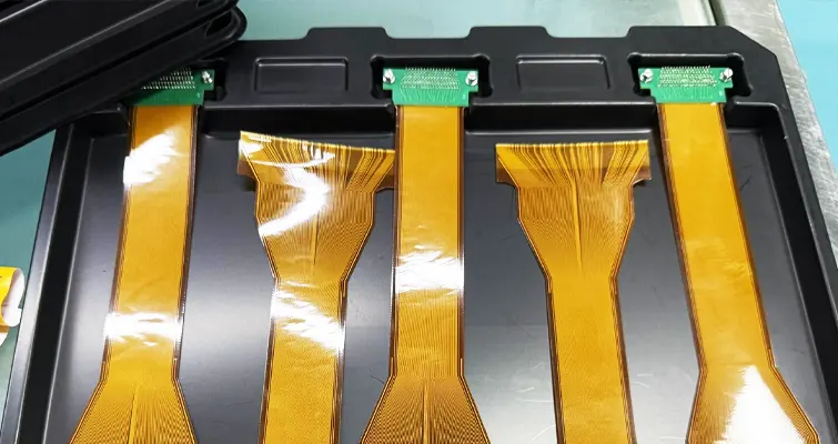
Flex PCB structure
Electrical Design Considerations in Flex Stackups
Electrical performance in flex PCB stackups is strongly influenced by layer ordering and dielectric consistency.
Controlled impedance traces require stable dielectric thickness and well-defined reference planes, which can be challenging in flexible constructions due to adhesive flow and material movement.
Signal integrity challenges unique to flex PCBs include impedance variation during bending, increased susceptibility to crosstalk, and difficulty maintaining continuous return paths.
Ground layers placed adjacent to high-speed signal layers improve impedance control and reduce EMI, but at the cost of increased stiffness.
For high-speed and high-frequency designs, adhesiveless stackups with thin dielectrics and closely coupled ground planes offer the most predictable performance.
Designers must also consider copper surface roughness and dielectric loss tangent, as these factors dominate insertion loss at multi-gigahertz frequencies.
Mechanical Design Considerations
Mechanical behavior of a flex PCB is governed by neutral axis theory, which states that strain is minimized at the neutral axis during bending.
Placing copper layers as close as possible to this axis reduces fatigue and extends flex life. Stackups with asymmetric layer placement experience higher stress on outer layers and are more prone to cracking.
Minimum bend radius is typically calculated as a multiple of total stackup thickness.
For dynamic bending, a conservative guideline is 10–15 times the total thickness, while static bending may tolerate 6–10 times the thickness. Increasing copper thickness or adding adhesive layers directly increases the required bend radius.
Stress concentration at cutouts, vias, and coverlay openings must be minimized through gradual transitions, filleted corners, and proper material selection.
Tear prevention strategies, such as reinforcement layers and grain-aligned copper routing, further enhance mechanical reliability.
Comparative Summary of Key Stackup Factors
| Stackup Factor | Impact on Performance |
|---|---|
| Thinner dielectric | Improved flexibility, higher flex life |
| RA copper | Superior fatigue resistance |
| Adhesiveless construction | Lower strain, better thermal stability |
| Ground plane proximity | Improved impedance control, reduced EMI |
| Balanced layer placement | Reduced stress concentration |
Thermal and Environmental Factors
Thermal behavior in flex PCB stackups differs fundamentally from that of rigid boards because flexible circuits lack the mass and heat-spreading capability of thick FR-4 laminates.
Heat dissipation in flex stackups relies primarily on copper layers acting as thermal paths rather than on the dielectric materials themselves.
As a result, copper thickness, plane continuity, and layer placement strongly influence temperature rise, particularly in power-carrying or densely routed designs.
Thermal expansion mismatch between layers is one of the most critical reliability considerations.
Polyimide exhibits a relatively low and stable coefficient of thermal expansion (CTE), while copper expands at a different rate, and adhesive layers—when present—often expand significantly more than either.
Under thermal cycling, especially in environments ranging from sub-zero to above 125 °C, this mismatch generates cyclic shear stress at material interfaces.
Over time, these stresses contribute to copper fatigue, adhesive degradation, and interfacial delamination.
For high-temperature or harsh environments, such as automotive engine compartments, aerospace systems, or industrial equipment, stackup design must prioritize material compatibility and thermal endurance.
Adhesiveless constructions, thinner dielectrics, and balanced copper distribution reduce thermally induced stress.
In extreme cases, designers intentionally limit layer count or isolate bend zones from high-temperature regions to preserve long-term reliability.
Manufacturability and Cost Optimization
Stackup decisions have a direct and often underestimated impact on manufacturing yield, lead time, and overall cost. Thinner stackups with fewer material interfaces generally offer higher yields due to reduced lamination complexity and tighter dimensional stability.
Conversely, multilayer flex stackups with adhesives, multiple lamination cycles, and complex via structures introduce cumulative tolerances that are difficult to control consistently.
Tolerance control becomes increasingly challenging as layer count increases. Variations in dielectric thickness, adhesive flow, and copper etching all stack together, affecting impedance, via registration, and coverlay alignment. These issues can lead to yield loss or extended process tuning, increasing both cost and lead time.
The primary cost drivers in flex PCB stackups are material selection, copper type, layer count, and overall structural complexity. Rolled annealed copper, adhesiveless substrates, and ultra-thin polyimide films carry higher raw material costs, while additional layers and vias increase processing time and inspection requirements.
Effective cost optimization therefore depends on eliminating unnecessary layers, minimizing copper thickness where electrically feasible, and selecting constructions aligned with actual mechanical and thermal requirements rather than conservative assumptions.
Design-for-manufacturing practices play a decisive role. Early collaboration with the manufacturer to validate material availability, achievable tolerances, and panel utilization can prevent late-stage redesigns. In many cases, modest adjustments to stackup thickness or layer ordering can significantly improve yield without compromising performance.
Typical Flex PCB Stackup Design Mistakes (and How to Avoid Them)
One of the most common stackup-related mistakes is incorrect copper type selection. Using electro-deposited copper in dynamic bend areas often leads to early fatigue failure, even when bend radius guidelines appear to be met. Selecting rolled annealed copper aligned with the primary bend direction dramatically improves endurance.
Another frequent error is designing overly thick stackups in an effort to increase robustness. In flex circuits, increased thickness almost always reduces flexibility and accelerates copper fatigue. Reliability is better achieved through optimized layer placement and material selection rather than added thickness.
Via placement across bend areas is a well-documented failure mechanism. Plated through-holes and stacked vias create rigid stress concentrators that crack under cyclic strain. Proper stackup design isolates vias to rigid or static zones and uses staggered via structures where multilayer flex is unavoidable.
Designers also often overlook manufacturing process constraints, assuming rigid PCB rules apply equally to flex.
Ignoring minimum lamination thicknesses, coverlay alignment tolerances, or achievable trace geometries leads to manufacturability issues that surface only during production ramp-up. These mistakes are avoidable through early DFM review focused specifically on flex processes.
Flex PCB Stackup Design Workflow (Step-by-Step)
An effective flex PCB stackup design workflow begins with a clear definition of both electrical and mechanical requirements. Signal speeds, current levels, impedance targets, bend locations, bend frequency, and environmental conditions must all be established before materials are selected.
Once requirements are defined, appropriate dielectric materials and copper types are chosen, balancing electrical performance against mechanical endurance.
Layer count and individual layer thicknesses are then determined to meet routing and impedance needs while maintaining acceptable flexibility. At this stage, total stackup thickness becomes a key design constraint.
The proposed stackup must then be validated mechanically by evaluating bend radius and neutral axis location.
This validation ensures copper layers experience minimal strain during bending and that dynamic flex life targets are achievable. Finally, a comprehensive DFM and DFA review with the manufacturer confirms that the stackup can be produced reliably at scale, with acceptable yield and cost.
This structured workflow significantly reduces late-stage design changes and improves first-pass success rates.
Industry Application Examples
In consumer electronics, particularly foldable devices and wearables, flex PCB stackups emphasize ultra-thin adhesiveless constructions with minimal copper thickness to achieve tight bend radii and long cycle life.
Electrical performance is often secondary to mechanical endurance, but high-speed interfaces increasingly require carefully controlled impedance even in these thin structures.
Automotive electronics, such as camera modules and distributed sensors, demand stackups that balance flexibility with thermal and vibration resistance.
Here, double-layer or rigid-flex stackups are common, with bend zones isolated from high-temperature regions and vias restricted to rigid sections.
Medical devices impose unique constraints. Implantable and diagnostic equipment require materials with proven biocompatibility, resistance to sterilization processes, and exceptional long-term reliability. Stackups are often conservative, favoring adhesiveless polyimide constructions and redundant mechanical margins.
Industrial and aerospace applications prioritize environmental resilience and predictable performance under extreme conditions. Flex PCB stackups in these sectors frequently integrate rigid-flex architectures, controlled impedance layers, and conservative bend designs to ensure reliability over long service lives.
Advanced Stackup Design Trends
Flex PCB stackup design is evolving rapidly in response to increasing functional density, higher signal speeds, and more demanding mechanical requirements. One of the most significant trends is the adoption of ultra-thin, high-density flex stackups that push total thickness below 50 µm for single-layer constructions and under 100 µm for complex rigid-flex interconnects.
These designs rely on adhesiveless polyimide laminates, ultra-thin rolled annealed copper, and tightly controlled coverlay systems to achieve small bend radii without sacrificing electrical performance.
At the same time, the boundary between flex and rigid-flex stackups is becoming increasingly blurred. High-speed digital interfaces and RF subsystems are now routinely integrated across rigid and flexible regions within a single stackup.
This integration places new demands on stackup continuity, impedance control across transitions, and thermal management. Designers must account not only for the flex region itself but also for how copper planes, reference layers, and dielectric thicknesses evolve across rigid-to-flex interfaces to avoid signal discontinuities and stress concentration.
Another emerging focus is reliability-driven stackup optimization. Rather than maximizing routing density or minimizing material cost alone, advanced designs prioritize fatigue life, thermal endurance, and environmental robustness as primary stackup objectives.
This approach leverages empirical failure data, accelerated life testing, and simulation to refine layer placement, copper thickness, and material selection. As a result, stackups are increasingly tailored to specific motion profiles, temperature ranges, and service lifetimes rather than relying on generic design rules.
Collaboration Between Designer and Manufacturer
Effective flex PCB stackup design cannot be achieved in isolation. Early collaboration between the designer and manufacturer is critical because many stackup constraints are process-dependent rather than purely theoretical.
Manufacturers possess practical knowledge of lamination behavior, material availability, achievable tolerances, and yield sensitivities that are not captured in design standards alone.
For accurate stackup development, manufacturers require detailed information including electrical performance targets, bend locations and cycle life expectations, environmental exposure conditions, assembly processes, and anticipated production volumes.
Without this data, stackup recommendations tend to be conservative, leading to unnecessary thickness, cost, or complexity.
Rapid prototyping plays a pivotal role in stackup validation. Producing early prototypes using production-intent materials and processes allows designers to verify bend performance, impedance stability, and assembly robustness before committing to volume production.
Feedback from these prototypes often leads to targeted stackup refinements that improve reliability while reducing cost. This iterative approach shortens development cycles and minimizes the risk of late-stage design changes.
Conclusion: Designing Flex PCB Stackups for Performance and Reliability
Flex PCB stackup design is a multidisciplinary engineering exercise that directly defines product reliability, electrical performance, and manufacturability.
Decisions related to material selection, copper type, layer ordering, and thickness are not independent optimizations; they form an interconnected system that governs how the circuit behaves under mechanical stress, thermal cycling, and long-term operation.
The key takeaway is that successful flex PCB stackups balance electrical requirements, mechanical endurance, and manufacturing realities from the earliest design stages.
Over-emphasizing any single factor—whether cost, flexibility, or signal integrity—inevitably compromises the others and increases lifecycle risk.
Organizations that engage flex PCB manufacturers early in the design process, treat stackup development as a collaborative effort, and validate assumptions through prototyping consistently achieve more robust and predictable outcomes.
In an era of increasingly compact, high-performance electronics, stackup design is no longer a background detail—it is a strategic engineering decision that determines whether a flex PCB meets its intended performance and reliability goals over its entire service life.

