Research on the Manufacturing Process of Semi-Rigid Flex Printed Circuit Boards


Semi-rigid printed circuit boards form a type of rigid-flex printed circuit board (R-FPCB). The conventional rigid board manufacturing process produces them by milling or cutting out openings (windows) in areas requiring flexibility.
They eliminate the need for expensive flexible materials like polyimide (PI), reducing costs while offering more stable electrical performance. These boards commonly serve in static or semi-dynamic bending applications to meet functional requirements.
Semi-flex printed circuit boards offer the following advantages:
- 1. Lower cost;
- 2. Excellent dimensional stability;
- 3. Space-saving bendable installation;
- 4. Reduced interface count during assembly for enhanced reliability.
Given these advantages, semi-rigid printed circuit boards represent an ideal choice for applications requiring only limited bending during installation and maintenance, where continuous dynamic bending is unnecessary. Using conventional rigid-flex boards in such scenarios would be overkill and excessively costly.
During semi-flexible R-FPCB production, depth-controlled milling creates semi-flexible zones. However, this process may result in uneven residual thickness, compromising bending performance.
When employing the windowing method, the bonding area is prone to concavity and semi-flex cracking risks during lamination, leading to poor film adhesion and subsequent circuit defects.
This study investigates two distinct processes for semi-flexible board fabrication to ensure timely, high-quality product delivery that meets customer requirements.
Product Specifications
Table 1 details the product specifications, and Figure 1 shows the laminate structure.

Figure 1 Product Layered Architecture

Table 1 Product Basic Information
Traditional Manufacturing Process for Semi-Rigid-Flex Boards
Materials
Manufactured using conventional FR4 core material for rigid layers and standard prepreg (PP) for semi-rigid layers.
Process Flow
Material Cutting → Inner Layer Pattern → Laminating → Drilling → Degumming → First Copper Plating → Outer Layer → Pattern Etching → Final Inspection → Solder Mask → Text Printing → Immersion Gold Plating → Controlled-Depth Milling → Forming.
Processing Issues and Post-Processing Problems
During controlled-depth milling of finished products, high precision in depth control is required. Uneven residual thickness affects flexural properties, with thickness variations prone to causing fractures, thereby compromising yield rates.
Improved Manufacturing Methods
Method 1
♦ Material Selection
Semi-rigid substrates serve the flexible zones, while conventional FR4 covers other rigid board areas. Low-flow prepregs fill the windowed areas, and conventional-flow prepregs fill the remaining areas.
♦ Laminate Structure Adjustment
The laminate structure follows a two-step lamination process:
During the second press, the prepreg for the flexible area windows and spacers fill and protect the flexible area. This reduces the difficulty of controlled-depth peeling in the finished product and prevents damage to the flexible area caused by controlled-depth peeling.
During lamination, 0.5–1.0 mm thick FR4 backing boards support both sides to prevent concavity in the bonding area or cracking of the flexible area. Figure 2 shows the stackup.

Figure 2 Secondary Press Fit Stacking Structure
♦ Process Flow
Material Cutting → L2 Layer Pattern → Primary Laminating → Other Inner Layer Patterns → Secondary Laminating → Drilling → Resin Removal → First Copper Plating → Outer Layer →
Pattern Printing → External Inspection → Solder Resist → Text Printing → Immersion Gold Plating → Controlled Depth Peeling → Forming.
♦ Final Product Results
After lamination, the flexible area remained intact without any indentation, resolving the outer layer circuit defect issue.
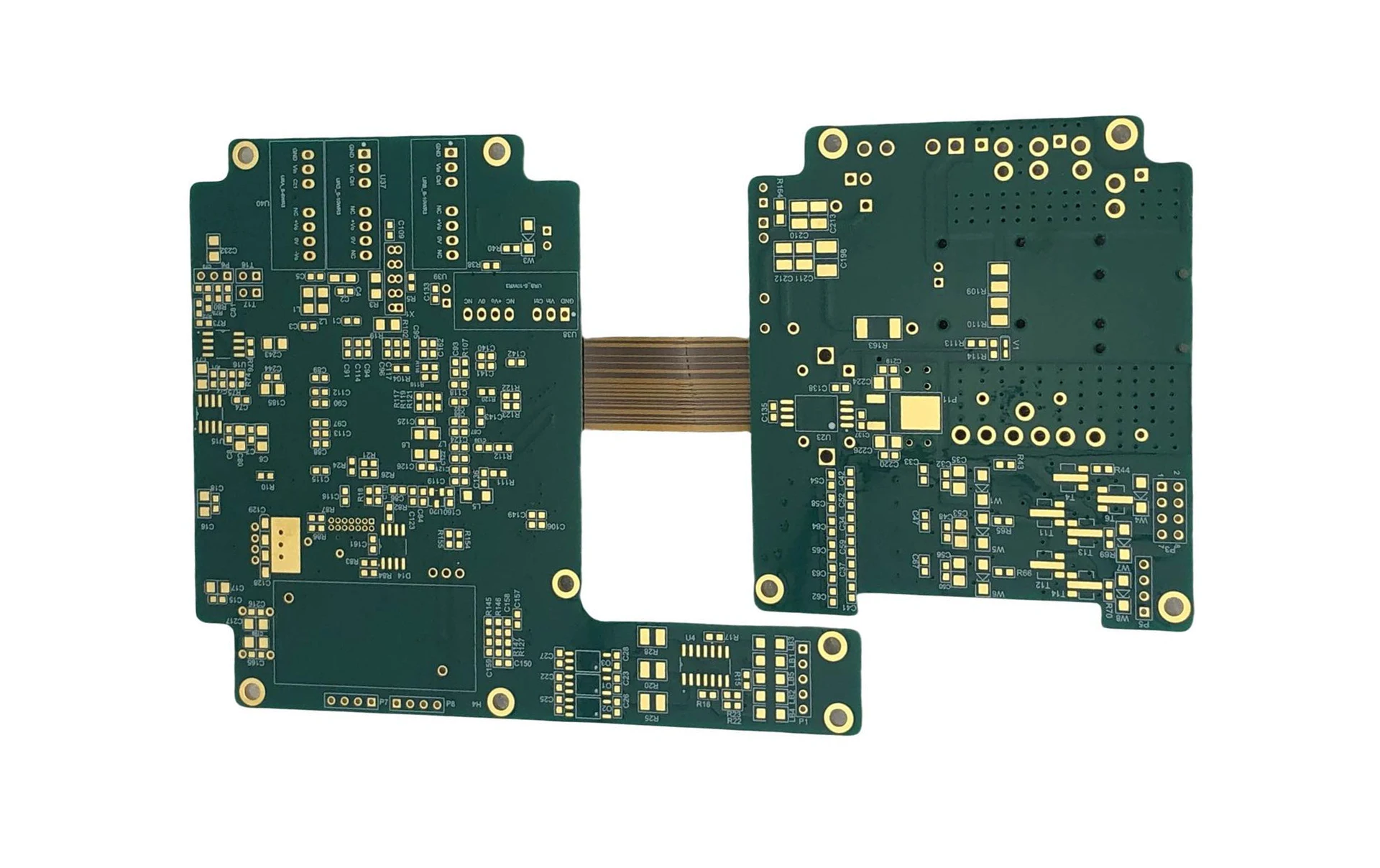
During controlled-depth de-capping, operational difficulty decreased significantly, and the semi-flexible area remained intact. Figure 3 shows the final product.

Figure 3: Semi-rigid Flex Rigid Printed Circuit Board Assembly
Method 2
♦ Material Selection
Flat glass fiber cloth with high fiber exposure served as the prepreg substrate, and the semi-rigid substrate was fabricated via bonding. Other materials followed the same procedure as Method 1.
♦ Laminate Structure Adjustment
The lamination process was adjusted to three pressing cycles. Compared to Method 1, this added only the pressing step for the semi-rigid substrate. Figure 4 shows the lamination structure for the semi-rigid substrate pressing.
The pressing process proceeded with the following parameters: heating rate 3–5 °C/min; material temperature 180 °C; dwell time 90 min; pressure 400–500 psi.

Figure 4: Semi-Flexible Substrate Laminated Sandwich Structure
♦ Process Flow
Step 1: Semi-flexible substrate preparation → Copper foil preparation → Laminating.
Step 2: Complete fabrication following the process flow of Method 1.
♦ Final Results
The flexible area remained intact after lamination with no indentation, preventing defects in outer-layer circuit formation. After controlled-depth stripping, the semi-flexible area remained undamaged. Figure 3 shows the finished product.
Reliability Testing
Thermal stress testing proceeded under the following conditions: immersion in a 288 °C tin bath for 10 seconds, repeated three times.
Cross-sections of 0.25 mm diameter holes revealed intact hole walls with no quality anomalies. Figure 5 shows the cross-section.

Figure 5: Cross-section of finished product after thermal stress testing
Comparison of Advantages and Disadvantages
Table 2 compares the advantages and disadvantages of different manufacturing processes for semi-rigid boards.

Table 2 Comparison of Advantages and Disadvantages of Different Manufacturing Methods for Semi-Rigid Boards
Conclusions
After selecting different semi-rigid materials and investigating processes—such as adding shims to prevent adhesive leakage during lamination and using depth-controlled lid removal for finished products—we drew the following conclusions:
(1) Using semi-rigid substrates with windowed prepregs over flexible zones and filling with shims carries risks of lamination indentation and cracking in the semi-rigid areas.
Adjusting the manufacturing process—specifically, using FR4 backing boards during lamination—can mitigate or prevent these issues.
This method offers advantages such as easier depth control and higher yield rates for finished products. However, few suppliers provide semi-flexible substrates, and procurement cycles take a long time.
Alternatively, fabricating prepregs using flat, high-open-end glass fiber cloth and bonding them into semi-flexible substrates adds only the lamination step compared to purchasing pre-made semi-flexible substrates. This approach effectively controls production cycles and reduces costs.
(2) Validation of both improved processes demonstrated their capability to produce qualified semi-rigid printed circuit boards.
Simultaneously, these methods reduce the difficulty of depth control during cover removal, preventing uneven residual thickness in flexible zones that could impair bending performance, thereby enhancing overall yield rates.
(3) This semi-rigid/flexible board fabrication successfully validated the processing techniques.
This process offers advantages, including a simplified workflow, user-friendly operation, low cost, and versatile implementation methods, meeting customer requirements for static or semi-dynamic bending applications.