PCB Copper Plating Process for Reliable Conduction


Introduction
Copper plating plays a crucial role in the production of PCBs. It ensures good electrical connections and strong mechanical support for printed circuit boards. These will create strong and stable traces. You can trust their quality even after bending or heat treatment.
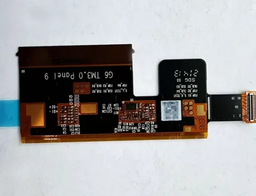
The copper plating process for flexible PCBs is like that for rigid PCBs. This article focuses on how copper plating is used in flexible PCBs.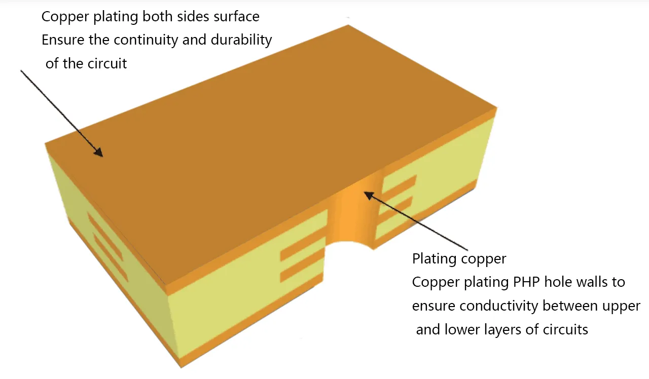
Modern rigid flex PCB designs are used in high-density applications. The plating process must meet strict design requirements. This ensures that all plated through-holes are fully conductive. Advanced pre-treatment methods, like the Black Hole process, help improve adhesion and uniformity. This is especially true for microvias and tricky via shapes.
This article explains the whole process of flexible PCB copper plating. It covers material preparations, the electroplating process, photo-imaged circuit patterning, quality checks, and real-world uses.
The Role of Copper Plating in Flexible PCBs
Copper plating provides a continuous electrical path across layers of flexible circuits. Its functions include:
- Strengthening copper traces for bending and flexing.
- Ensuring reliable conductivity in plated through holes.
- The design combines flexible and rigid layers to support rigid flex plating.”
- Enabling high-density layouts without signal loss.
Furthermore, copper plating also influences the long-term reliability of the board. Poor plating may result in the form of open circuits, signal loss, or mechanical failure. Engineers use professional electroplated copper or rolled annealed copper for applications that require repeated bending and harsh conditions.
Reference: DuPont Flexible Circuit Materials
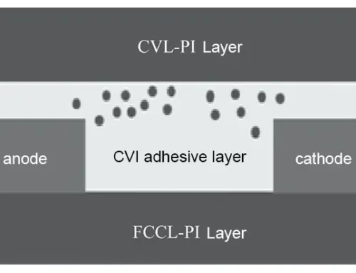
Pre-Treatment and Black Hole Process
Before plating, holes must be prepared. Traditional methods employ electroless copper, which chemically deposits a thin seed layer.
The VIA walls have a carbon-based conductive layer. This layer is made using a process called Black Hole, which combines physical adsorption and chemical bonding. Although not required, this can help decrease defects and better plating adhesion, especially for microvias and high-density designs.
Even for the Black Hole, the focus is on the flexible PCB copper plating process. It also features strong plated-through holes and surface copper traces.
Step-by-Step Copper Plating Process
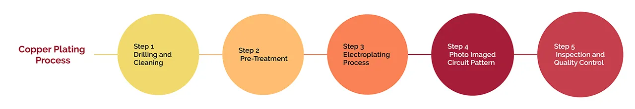
Step 1 – Drilling and Cleaning
Holes are drilled in the substrate material (typically polyimide films) and cleaned thoroughly. The PCB cleaning process removes debris, resin smears, and contaminants. Proper material preparations ensure uniform plating and strong adhesion in subsequent steps.
Step 2 – Pre-Treatment
Pre-treatment may include electroless copper or the Black Hole process for enhanced adhesion. This step is critical to ensure all plated through holes are conductive and ready for copper deposition.
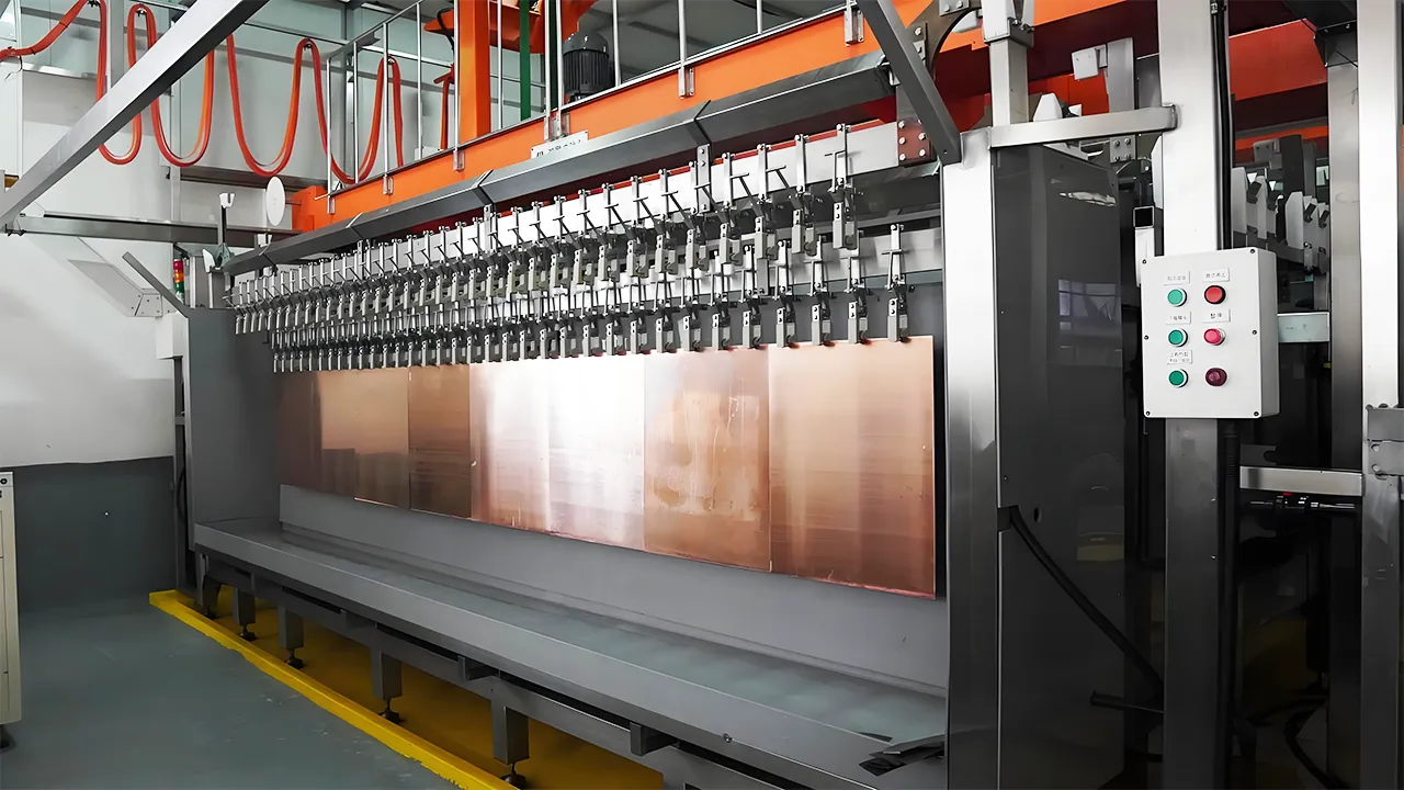
Step 3 – Electroplating Process
The electroplating process deposits copper onto the prepared surfaces. Engineers control copper thickness to meet both electrical and mechanical requirements. For flex circuits, rolled annealed copper is best for bending areas because it is flexible. On the other hand, electro-deposited copper works well in rigid areas with fine circuit patterns.
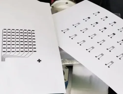
Step 4 – Photo Imaged Circuit Pattern
A photo-imaged resist defines the circuit pattern on surfaces, ensuring only designated areas receive copper plating. This step is critical for achieving high-density layouts without short circuits.
Step 5 – Inspection and Quality Control
Inspection verifies:
Continuity of all plated through holes.
Correct copper thickness across the board.
Absence of voids or peeling.
Quality control ensures that rigid flex PCBs and flexible circuits perform reliably in demanding applications.
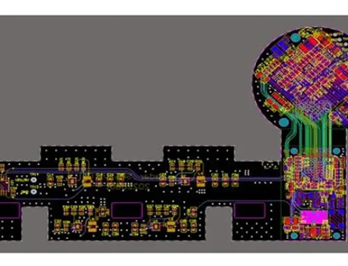
Design and Manufacturing Considerations
Careful design and manufacturing practices enable more effective flexible PCB copper plating.
- Stack: Layered structures had to be platable without delaminating.
- Copper thickness: If the copper plating is too thick, it can be hard to bend. If it is not thick enough, it can affect conductivity.
- Circuit pattern: Fine-pitched can afford the finest control of plating to avoid shorts.
- Plating process parameters: Optimize current density, temperature, and agitation for best results.
- Adhesion improvement: The Optional Black Hole process can enhance reliability in microvias.
Manufacturers often do small tests on flexible printed circuit boards. They do this to improve the electroplating process before starting full production.
Reference: IPC-6013 Flexible/Rigid-Flexible Printed Boards Standard
Common Challenges and Solutions
| Problem | Cause | Solution |
|---|---|---|
| Poor adhesion | Incomplete cleaning | Improve PCB cleaning process |
| Voids in plated holes | Uneven plating | Adjust the electroplating process parameters |
| Over-thick copper | Excess plating | Control copper thickness |
| Cracking in flex regions | High copper stiffness | Use rolled annealed copper and optimize circuit design |
Additional tips:
Monitor current density to avoid over-deposition in critical vias.
Inspect the material stack for defects before plating.
Use photo-imaged resist carefully to maintain precise circuit patterns.
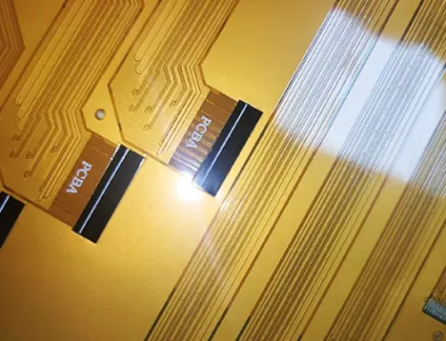
Applications of Flexible PCB Copper Plating
Flexible PCB copper plating serves many industries:
Foldable devices and wearables rely on flex circuits with dependable plated through-holes, as do consumer electronics
Sensors, lighting, and control modules need to have copper traces that can stand up to automotive use
Medical equipment: The monitoring unit requires a precise design to fit into a small space. It uses a high-quality rigid flex PCB.
Aerospace & Defense: These dense and strong types of flexible PCBs can resist vibration and thermal stresses.
Correct plating will ensure reliable operation in applications where repeated bending or exposure to harsh environments is required.
Advantages of Proper Copper Plating
Reliable electrical connectivity for plated through holes and surface copper traces.
Uniform copper thickness across the board.
Supports high-density layouts with minimal defects.
Compatible with electro-deposited copper, rolled annealed copper, and optional Black Hole pre-treatment.
Ensures design and manufacturing compliance for modern electronics.
Future Trends and Considerations
As flexible circuits continue to evolve, copper plating technologies must adapt:
Smaller via sizes demand improved via plating techniques.
Higher-density circuits require precise control of copper traces and plated through-holes.
Environmentally friendly alternatives like the Black Hole process may reduce chemical waste while maintaining performance.
Advanced rigid flex PCB designs will integrate more flexible layers, increasing reliance on consistent copper plating.
Engineers and manufacturers should continuously optimize electroplating process parameters, circuit patterns, and material stacks to meet evolving design requirements.
Conclusion
Without proper copper plating on flexible PCBs, you cannot build a reliable flex circuit or rigid flex PCB board. Before treatment, the electroplating process helps create reliable copper traces. Panel-plated micro vias and photo-imaged circuit patterning also contribute to this. Together, they ensure fully conductive plated through holes.
Engineers can use these best practices to create flexible circuits. These circuits meet the high demands of today’s consumer, automotive, medical, and aerospace electronics.
Other post:
FAQ:
1. Why is copper plating important in flexible PCB manufacturing?
Copper plating ensures reliable electrical connections and mechanical strength across all circuit layers. It strengthens copper traces, supports bending and flexing, and maintains conductivity in plated through-holes—essential for durable and high-performance flexible PCBs.
2. How is copper plating in flexible PCBs different from rigid PCBs?
While the basic process is similar, flexible PCB plating must account for bending stress and thermal expansion. Flexible PCBs often use rolled annealed (RA) copper for flexibility, while rigid boards use electro-deposited (ED) copper for precision. Rigid-flex designs combine both to balance strength and flexibility.
3. What is the “Black Hole” process in copper plating?
The Black Hole process is a carbon-based pre-treatment that coats via walls with a conductive layer. It enhances copper adhesion and uniformity—especially for microvias and high-density designs—by combining physical adsorption with chemical bonding. It’s an environmentally friendly alternative to traditional electroless copper methods.
4. What are the main steps in the flexible PCB copper plating process?
Drilling and cleaning – Prepare the substrate and remove debris.
Pre-treatment – Use electroless copper or the Black Hole process.
Electroplating – Deposit controlled copper thickness.
Photo-imaged circuit patterning – Define copper trace areas.
Inspection and quality control – Verify thickness, adhesion, and continuity.
5. What materials are used for copper plating in flexible PCBs?
Engineers commonly use:
Rolled Annealed (RA) Copper for bending and dynamic flexing zones.
Electro-Deposited (ED) Copper for rigid and fine-pitch areas.
These materials ensure both mechanical resilience and high conductivity.
6. How is copper thickness controlled during plating?
Copper thickness is regulated by electroplating current density, bath temperature, and time. Too much copper can make the PCB difficult to bend, while too little reduces conductivity. Manufacturers follow IPC-6013 standards to ensure consistency.
7. What quality control methods are used in copper plating?
Quality checks include:
Measuring copper thickness uniformity
Microscopic inspection for voids and cracks
Adhesion tests for peel strength
Continuity testing for plated through-holes
These ensure reliability under bending, heat, and vibration.
8. In which industries is flexible PCB copper plating widely used?
Copper-plated flexible PCBs are used in:
Consumer electronics – foldable devices, wearables
Automotive – sensors, lighting, control systems
Medical devices – compact monitoring units
Aerospace and defense – vibration- and heat-resistant circuits
9. What are the latest trends in flexible PCB copper plating?
Miniaturized vias require more precise plating control.
Black Hole pre-treatment reduces chemical waste.
Hybrid rigid-flex designs increase plating complexity.
Process optimization improves conductivity and reduces defects.
These advancements support next-generation flexible circuits in high-density and eco-friendly applications.